Low contact resistivity between Ni/Au and p-GaN through thin heavily Mg-doped p-GaN and p-InGaN compound contact layer

Low contact resistivity between Ni/Au and p-GaN through thin heavily Mg-doped p-GaN and p-InGaN compound contact layer |
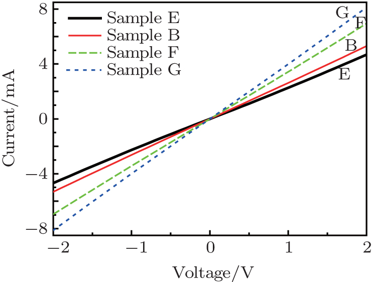
| CTLM I – V measurement for four samples with different Cp2Mg flow rates when the spacing of the CTLM pattern is fixed as 30 μm at room temperature. |
 |