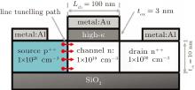
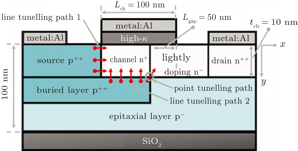
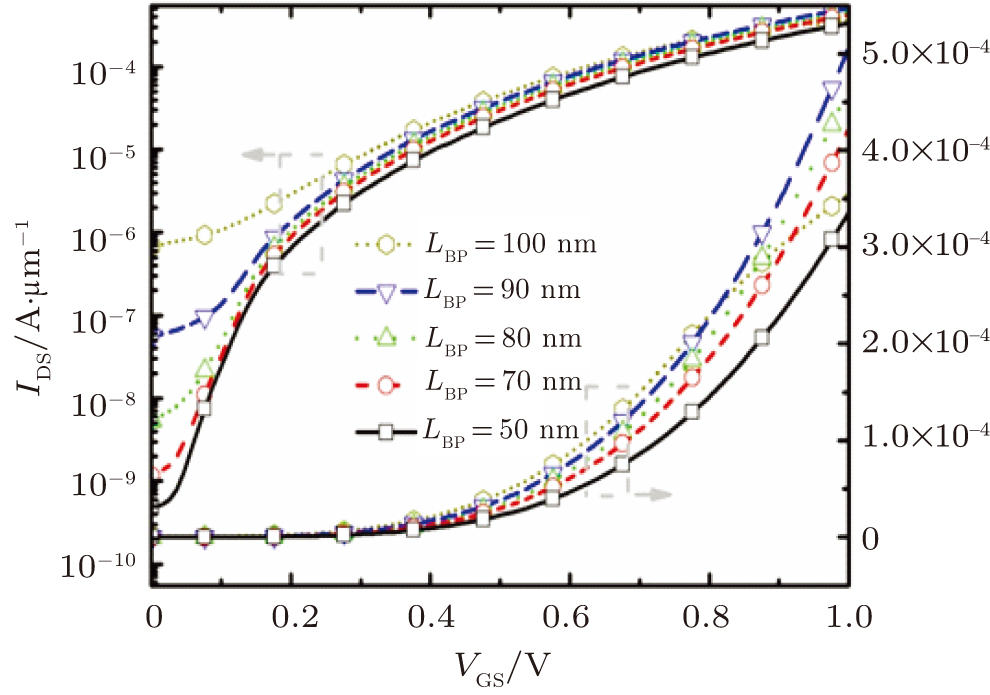
| [1] |
Benneventi G B, Gnani E, Gnud A, Reggianii S, Baccarani G 2015 IEEE Trans. Electron Dev. 62 44 DOI: 10.1109/TED.2014.2371071 |
| [2] |
Mallikarjunarao, Ranjan R, Pradhan K P, Artola L, Sahu P K 2016 Superlattices Micro. 97 70
|
| [3] |
|
| [4] |
Aslam M, Yadav S, Soni D, Sharma D 2017 Superlattices Micro. 112 86
|
| [5] |
|
| [6] |
|
| [7] |
|
| [8] |
Soni D, Sharma D, Yadav S, Aslam M, Sharma N 2018 Superlattices Micro. 113 94
|
| [9] |
|
| [10] |
|
| [11] |
Wang W, Wang P F, Zhang C M, Lin X, Liu X Y, Sun Q Q, Zhou P, Zhang D W 2014 IEEE Trans. Electron Dev. 61 193 DOI: 10.1109/TED.2013.2289075 |
| [12] |
|
| [13] |
|
| [14] |
|
| [15] |
Singh B, Rai T, Gola D, Singh K, Goel E, Kumar S, Tiwari P, Jit S 2017 Materials Science in Semiconductor Processing 71 161 DOI: 10.1016/j.mssp.2017.07.014 |
| [16] |
Low K, Zhan C, Han G, Yang Y, Goh K, Guo P, Toh E, Yeo Y 2012 Jpn. J. Appl. Phys. 51 02
|
| [17] |
Mitra S, Goswami R, Bhowmick B 2016 Superlattices Micro. 92 37
|
| [18] |
|
| [19] |
|
| [20] |
|
| [21] |
Avci U, Chu-Kung B, Agrawal A, Dewey G, Le V 2015 IEEE International Electron. Dev. Meeting December 7–9, 2015 Washington DC, USA 891
|
| [22] |
Krishnamohan T, Kim D, Raghunathan S, Saraswat K 2008 IEEE International Electron. Dev. Meeting December 15–17, 2008 San Francisco, USA
|
| [23] |
Zhang Q, Sutar S, Kosel T, Seabaugh A 2009 Solid-State Electrons 53 30
|
| [24] |
Takagi S, Kim W, Jo K, Matsumura R, Takaguchi R, Katoh T, Bae T, Kato K, Takenaka M 2018 ECS Trans. 86 75
|
| [25] |
Katoh T, Matsumura R, Takaguchi R, Takenaka M, Takagi S 2018 Jpn. J. Appl. Phys. 57 04
|
| [26] |
Matsumura R, Katoh T, Takaguchi R, Takenaka M, Takagi S 2018 Jpn. J. Appl. Phys. 57 04
|
| [27] |
Liu X, Hu H Y, Wang B, Wang M, Han G, Cui S, Zhang H M 2017 Superlattices Micro. 102 7
|
| [28] |
|
| [29] |
Colinge J P, Lee C W, Afzalian A, Akhavan N, Yan R, Ferain I, Razavi P, O’Neil B, Blake A, White M, Kelleher A, McCarthy B, Murphy R 2010 Nat. Nanotechnol. 5 225 DOI: 10.1038/nnano.2010.15 |
 ), Sheng Hu(胡晟)1, Yue Feng(冯越)1, Peng Li(李鹏)2, Hui-Yong Hu(胡辉勇)1, Bin Shu(舒斌)1