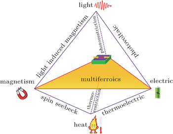
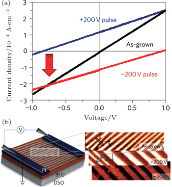
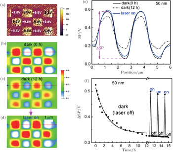
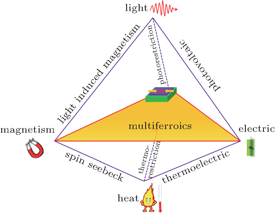
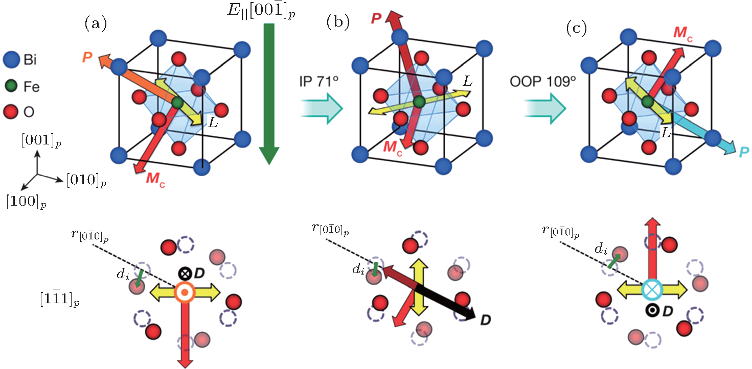
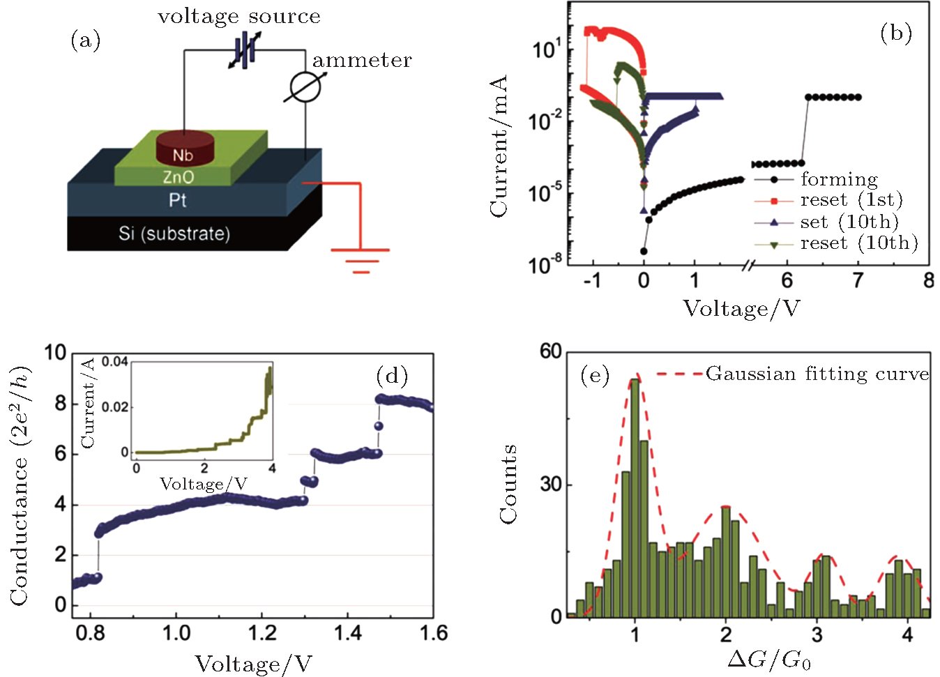
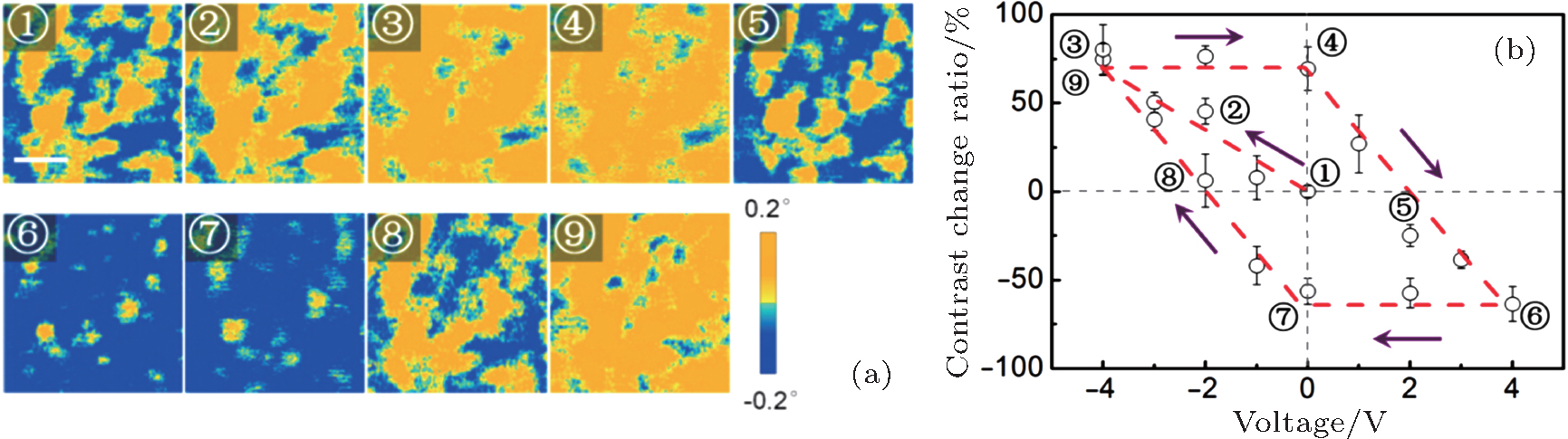
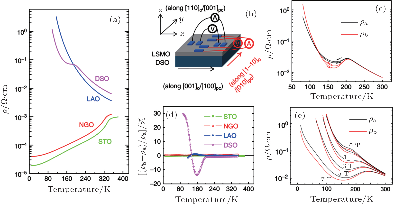
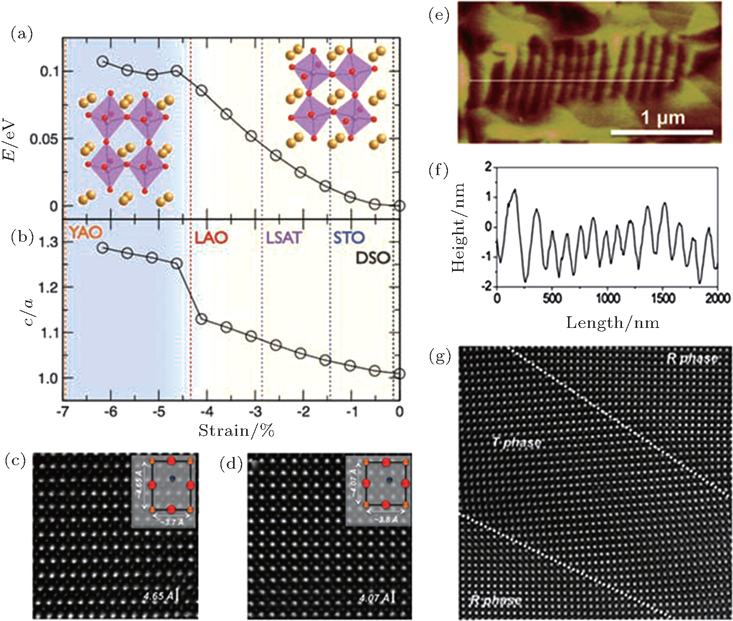
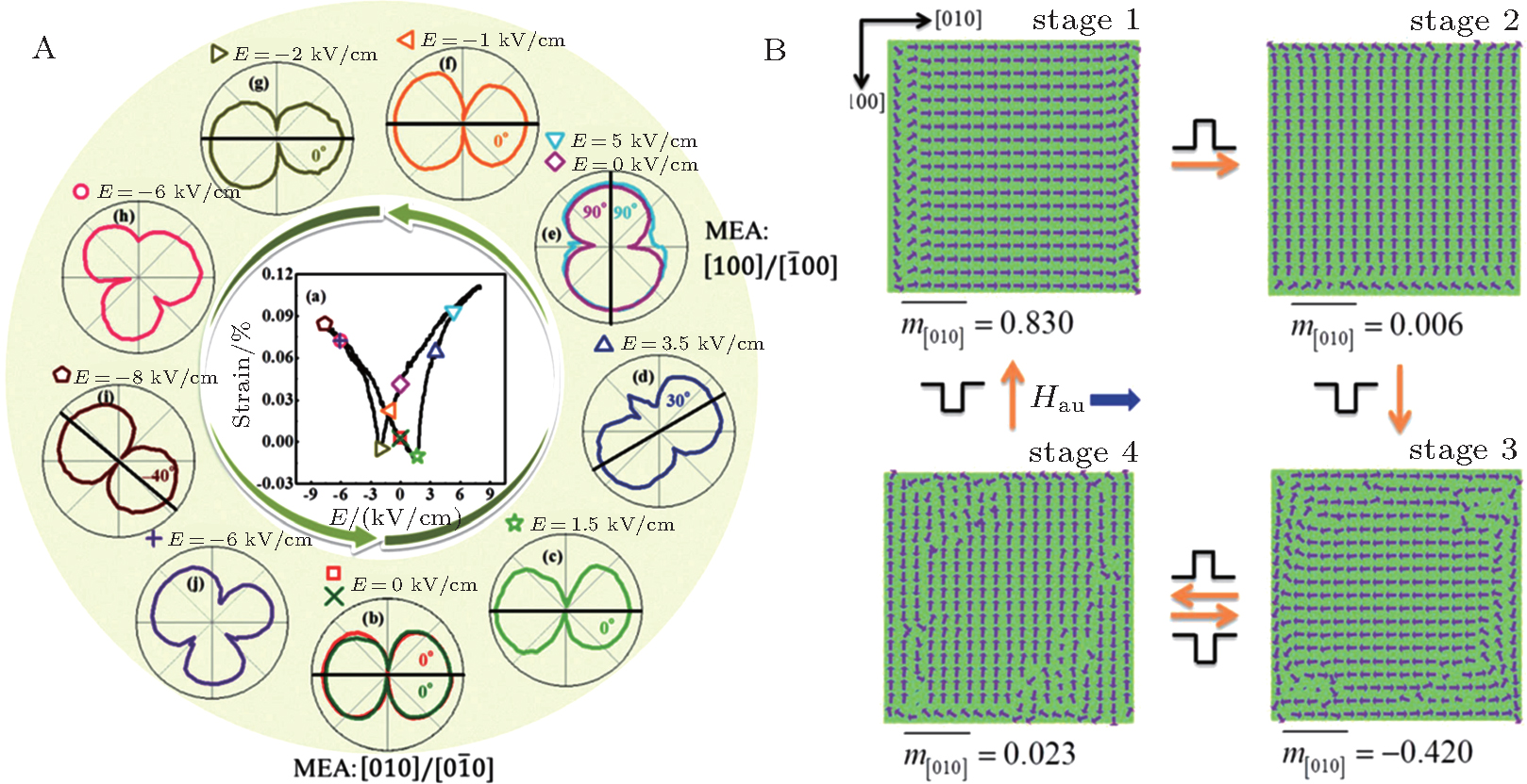
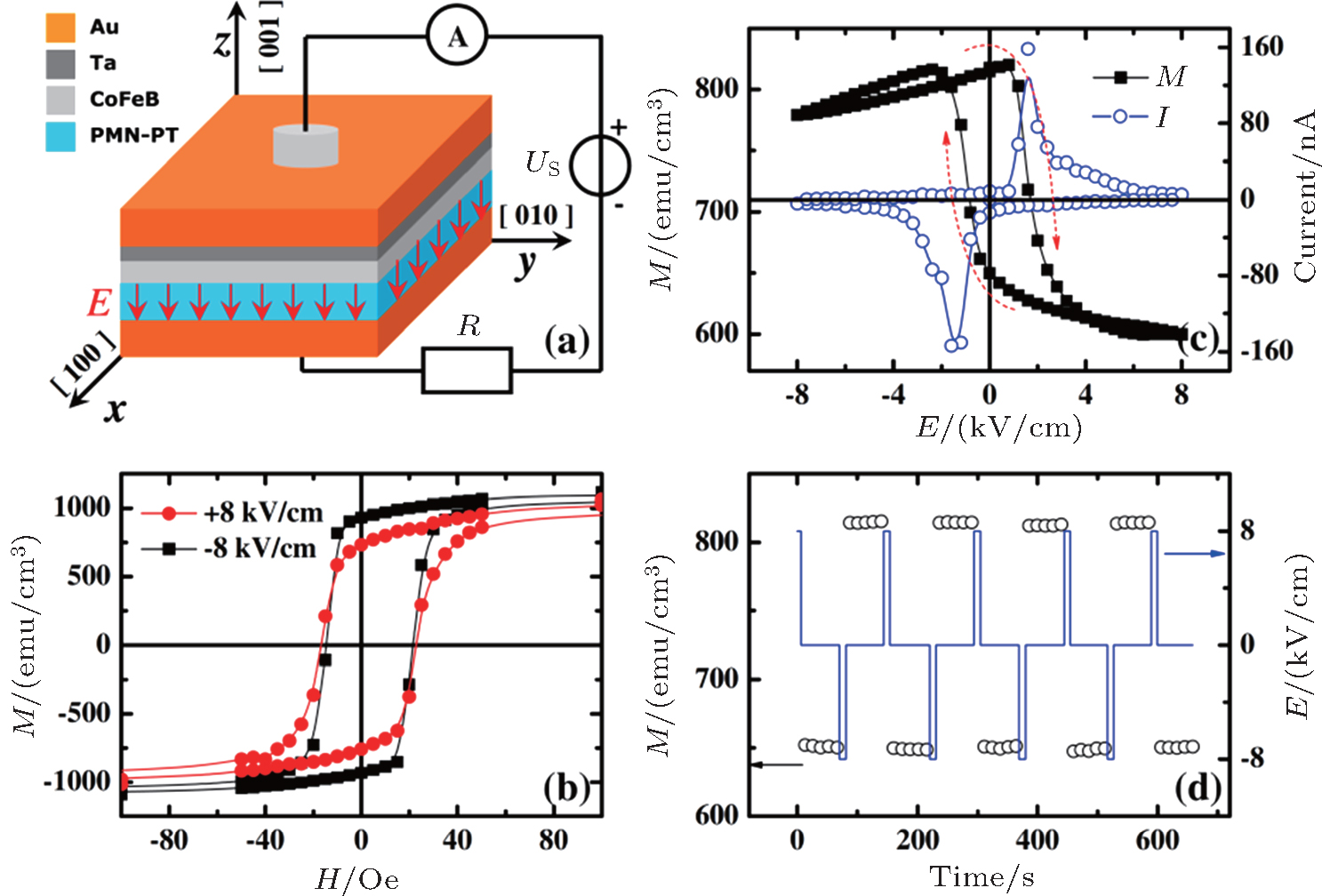
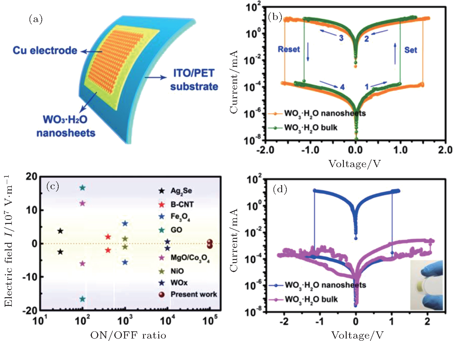
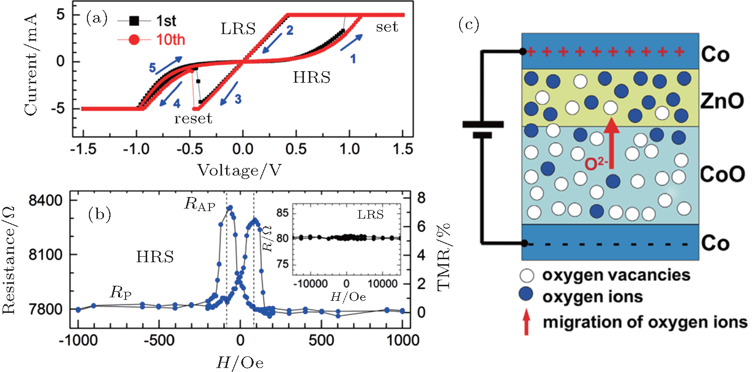
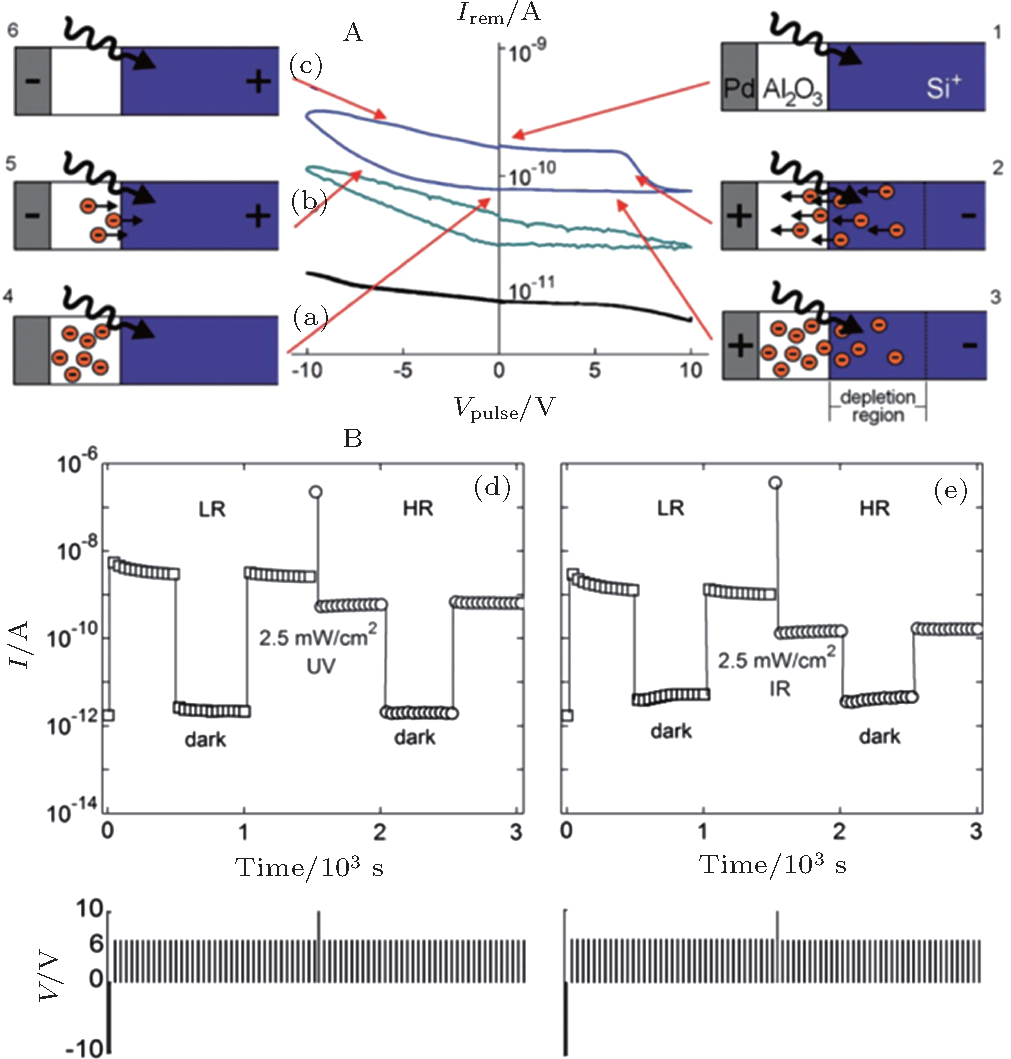
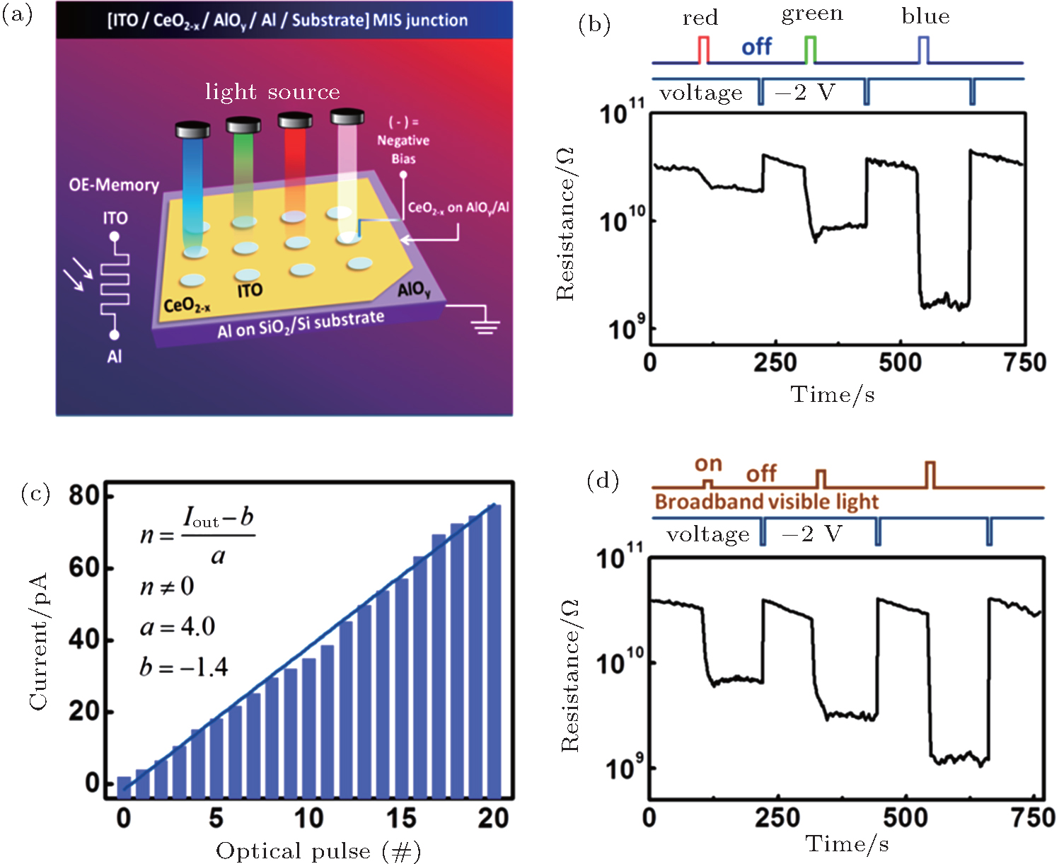
Modulation of physical properties of oxide thin films by multiple fields
Yang Hua-Li1, 2, Wang Bao-Min1, 2, †, , Zhu Xiao-Jian1, 2, Shang Jie1, 2, Chen Bin1, 2, Li Run-Wei1, 2, ‡,
Key Laboratory of Magnetic Materials and Devices, Ningbo Institute of Materials Technology and Engineering, Chinese Academy of Sciences, Ningbo 315201, China
Laboratory of Magnetic Materials and Application Technology, Ningbo Institute of Materials Technology and Engineering, Chinese Academy of Sciences, Ningbo 315201, China


† Corresponding author. E-mail: wangbaomin@nimte.ac.cn

‡ Corresponding author. E-mail: runweili@nimte.ac.cn

Project supported by the State Key Project of Fundamental Research of China (Grant No. 2012CB933004), the National Natural Science Foundation of China (Grant Nos. 11474295, 51571208, 51525103, and 11274322), Overseas, Hong Kong & Macao Scholars Collaborated Researching Fund (Grant No. 51428201), the Instrument Developing Project of the Chinese Academy of Sciences (Grant No. YZ201327), Ningbo Major Project for Science and Technology (Grant No. 2014B11011), Ningbo International Cooperation Projects (Grant Nos. 2012D10018 and 2014D10005), the Fund for Ningbo Science and Technology Innovation Team (Grant No. 2015B11001), the Youth Innovation Promotion Association of the Chinese Academy of Sciences, and the Key Research Program of the Chinese Academy of Sciences (Grant No. KJZD-EW-M05).

Abstract
Abstract

Recent studies of the modulation of physical properties in oxide thin films by multiple fields are reviewed. Some of the key issues and prospects of this area of study are also addressed. Oxide thin films exhibit versatile physical properties such as magnetism, ferroelectricity, piezoelectricity, metal–insulator transition (MIT), multiferroicity, colossal magnetoresistivity, switchable resistivity. More importantly, the exhibited multifunctionality can be tuned by various external fields, which has enabled demonstration of novel electronic devices.

PACS: 73.23.–b;73.50.Pz;77.55.Nv
1. Introduction

Oxides are a class of materials that are particularly attractive due to their remarkable physical properties and multifunctionality.[14] For example, a diversity of physical properties exhibited in thin film oxides, such as magnetism, ferroelectricity, piezoelectricity, and superconductivity, have been intensively studied in the past several decades,[510] and the interplay between them has become a hot topic in condensed matter physics.[1115] Intriguing phenomena including MIT,[1624] colossal magnetoresistivity,[2529] resistive switching,[3038] ferroelectricity,[3945] multiferroicity,[4656] etc., make oxides appealing candidates for both electronic and spintronic devices.[5763] From a fundamental perspective, the multifunctionality in oxides provides a playground for investigating the interplay between spin, charge, orbital and lattice degrees of freedom.[24,6467] A number of interesting phenomena such as charge order, orbital order, multiferroicity, and interactions such as the electron correlation effect, Jahn–Teller interaction, and spin-orbit coupling, have been frequently discussed to understand the fundamental physics.[51,64,6873] In addition, the advent of atomically tailored oxide heterostructures has enabled the observation of emergent phenomena, and raised excitement in the study of novel phenomena due to the symmetry breaking and charge transfer across the oxide interface.[67,7376]

The interplay between spin, charge, orbital, and lattice degrees of freedom in oxides (especially complex oxides) reveals strong composition-structure-property relationships, and it enables study of the effects of various types of fields in various combinations on the physical properties of thin film oxides. As shown in Fig. 1, the interconnections between light, magnetism, heat, strain, and electric has been demonstrated in condensed matters, and many novel phenomena such as photorestriction,[77] thermal spin-transfer torque,[78] and multiferroicity have been revealed in functional oxides. Many novel devices with multifunctionality have been proposed, such as spin-resistive random access memories (RRAM), electric operational magnetic random access memories (MRAM), multiferroic tunnel junctions, etc.

Fig. 1. Schematic showing the various fields (light, magnetism, heat, electric, and strain) modulating the physical properties in oxides.

In many cases, combined external stimuli could enable fine tuning of physical properties in thin film oxides, which could benefit practical applications. In the following paragraphs, we will discuss the response of thin film oxides to an external stimulus such as electrical field, strain field, magnetic field or photo illumination. We have focused special concern on multiferroics, perovskite manganites, and oxides with resistive switching (RS) properties.

2. Electric field effect

Electric field has been recognized as an efficient and scalable way to tune the physical properties in various materials and structures. For example, in magnetic tunneling junctions, a spin polarized current can induce spin transfer torque effect, which has been intensively studied in MRAM devices[7982] and microwave devices.[83] Upon the application of electric field, the polarization direction of ferroelectrics can be switched. This can result in either a large electroresistance effect in ferroelectric tunnel junctions[84,85] or a switchable diode effect in ferroelectric diodes.[86] Noticeable strain effect associated with electric-field-induced ferroelastic domain switching has also been intensively studied in magnetoelectric heterostructures.[87,88] In multiferroic materials where the electric polarization couples with the magnetization, applying an electric field modifies the electric polarization and tunes its magnetization through the magnetoelectrical (ME) coupling effect.[11,89,90] In RRAM devices, applying an electric field induces the RS effect by associating with several electric-field-induced effects: electric field induced ion transport,[35] electric field induced phase transition,[91] and the Joule heating effect.[92]

2.1. Electric field control of magnetism

The interplay between electric polarization and magnetization has attracted wide interest for applications such as spintronic devices.[48,93] The presence of multiferroicity in some materials and structures has enabled several ways for the magnetic properties to be manipulated by applying an electric field:[94] (i) In single phase multiferroics where magnetic order and ferroelectricity are coupled, applying an electric field can alter the electric polarization along with the magnetization, owing to intrinsic ME coupling.[11] (ii) Many multiferroics are antiferromagnets; by attaching a multiferroic layer to a ferromagnetic layer, it is possible to construct an exchange bias system that can be controlled by applying electric field to the multiferroic layer, which is known as exchange-mediated ME coupling effect.[12] (iii) In magnetoelectric composites composed of ferroelectric (FE)/ferromagnetic (FM) heterostructures,[95] applying an electric field in the FE layer induces strain that is transmitted in to the FM layer and changes its magnetic properties through inverse magnetostrictive effect. (iv) In FE/FM heterostructures, the electric field can also switch the polarization direction of the FE layer, which may tune the carrier density and hence the magnetic properties of the FM layer, a phenomenon called charge-mediated ME coupling effect.[96]

In single phase multiferroic materials, a tempting idea is to design multiferroics that combine both ferromagnetism and ferroelectricity, and the manipulation of its magnetization by an electric field would be essential for the magnetoelectric control of spintronic devices. However, the exploration of ferromagnetism and ferroelectricity together in a single phase multiferroic has been found unexpectedly difficult.[46] One promising single phase multiferroic that could be utilized is BiFeO3 (BFO) — a material that unambiguously shows ferroelectricity and anti-ferromagnetism above room temperature.[97] The principle that BFO can be utilized for efficient magnetoelectric control of spintronic devices relies on the possibility of electric field controlled interfacial coupling composed of a BFO layer and a ferromagnetic layer.[12,98,99]

Recently, Heron et al. demonstrated deterministic magnetization reversal in BFO based heterostructures,[99] by utilizing the coupling between its weak magnetization arising from the Dzyaloshinskii–Moriya (DM) interaction and the ferroelectric polarization,[100,101] as well as the strong interfacial magnetic coupling.[102] Earlier, theory had predicted[103] that the direct reversal of ferroelectric polarization in BFO will leave the orientation of the canted magnetic moment unchanged, Heron et al. found that ferroelectric-polarization reversal in a strained BFO film actually follows an indirect pathway, and proposed that the indirect switching path reverses the canted magnetic moment [Fig. 2]. The ME coupling is determined by the DM interaction, where the weak ferromagnetism Mc is determined by the DM vector given by D ∼ Σdi × ri, where ri is a constant vector that connects neighboring Fe3+ ions and di is the displacement of the intermediate oxygen atom from the mid-point of ri caused by the O6-rotation. Since the in-plane 71° and out-of-plane 109° switches are found to be capable of rotating D and the associated Mc by 90° [Figs. 2(b) and 2(c)], the reversal of D through the sequential in-plane 71° and out-of-plane 109° switches would also be expected to reverse Mc. Furthermore, they deposited a spin valve structure on top of the strained BFO and realized the electric-field control of a spin-valve device at room temperature.

Fig. 2. (a) A domain with polarization P initially along the (111). L represents the antiferromagnetic axis. O6 rotations are shown with respect to an octahedron that is not rotated (dashed circles). (b) After an in-plane 71° switch. E represents the applied electric field. (c) After an out-of-plane 109° switch.[99]

Progress in strain-mediated and charge-mediated ME effect will be further discussed in later sections.

2.2. Electric field induced ion migration

RRAM has been widely investigated for next-generation nonvolatile memory devices due to its simple structure, high density, low power consumption and compatibility with complementary metal oxide semiconductor technology.[61,104106] Up to now, a large variety of materials have been investigated for RS, including solid electrolytes,[107] perovskite oxides,[32,108110] binary oxides,[33,35,37,111] organic materials,[112114] amorphous silicon,[115] and amorphous carbon.[116] Although the underlying mechanism is still controversial due to the diversity of RS behaviors, the conductive filament (CF) model has gained much success and has been accepted extensively.[34]

RRAM devices have a simple metal-insulator-metal sandwiched structure. For filament model based RRAMs, a sufficiently large electrical field between the two metallic electrodes can induce a soft dielectric breakdown in the insulator and set the device to a conductive state (also called an ON-state). In this process, due to the electrically induced ion migration, a large number of defects are formed inside the film and form CFs that connect the two terminal electrodes. The ON-state can also be electrically reset, leading to the OFF-state that corresponds to disruption of the CFs. In the CF model, the formation and rupture of local conducting paths connecting the two-terminal electrodes dominates the RS process.[36,38,117,118] Liu et al. have performed real-time characterizations of the CF formation and dissolution processes of an oxide-electrolyte-based RRAM device[36] that is based on a vertical Ag(Cu)/ZrO2/Pt structure with both small lateral sizes and ZrO2 thickness to facilitate direct TEM studies. During the SET process, a dark nano-bridge region appears, signifying the formation of CF [Fig. 3(a)]. Successive RESET process has been performed, and a first RESET voltage sweep is found to decrease the electrical current passing through the device drastically [Fig. 3(b)]. Meanwhile, the CF region near the Pt electrode was substantially weakened after the first RESET process [Fig. 3(c) and 3(d)]. The chemical compositions of the CF region in the initial-, ON- and OFF-states were analyzed using energy-dispersive x-ray spectroscopy (EDX) analysis and are found to be Ag in the Ag/ZrO2/Pt device [Fig. 3(e)]. These experiments have led to intuitive, more complete understanding of the underlying nature of the RS behavior and the corresponding CF evolution process.

Fig. 3. (a) IV curve of the Ag/ZrO2/Pt TEM specimen during SET operation. Inset is a TEM image of the specimen after the SET process. (b) IV curves of the TEM specimen under successive RESET operations. (c) High resolution TEM image of the CF region in an Ag/ZrO2/Pt TEM specimen after SET process. (d) High resolution TEM images showing that the CF dissolves from the anode (Pt) to the cathode (Ag) terminal during RESET voltage sweeps (0 → 1.5 V). (e) EDX analysis of the TEM specimen conducted at the initial-, ON- and OFF-states.[36]

It has been found that the nanoscale conduction channel not only dominates the RS process but also shows some other effects, such as quantum size effects and exchange bias effect. For example, quantized conductance has been realized in zinc-oxide based sandwich devices.[35] As can be seen from Fig. 4, the Nb/ZnO/Pt device shown in Fig. 4(a) can be Set and Reset repeatedly, exhibiting typical bipolar RS behaviors [Fig. 4(b)]. During the Set process where the nanoscale conducting channel is forming, the conductance shows quantum behavior corresponding to electron travelling along the nanoscale channel [Fig. 4(c) and (d)]. Similar phenomena have also been found in other sandwiched thin films.[118122]

Fig. 4. (a) Schematic of a sandwiched Nb/ZnO/Pt structure. (b) Typical bipolar RS behaviors observed in the device. (c) Measured conductance as a function of the bias voltage during the set process. Inset: Corresponding IV curve in a larger voltage range from 0 V to 4 V. (d) Histogram of the conductance changes ΔG obtained from the forming and set processes.[35]

It has also been revealed that by controlling the migration of ions through electrical fields, the magnetism of some magnetic dielectrics can be modulated. For example, Chen et al. successfully modulated the magnetization and coercive field of Co-doped ZnO thin films.[123] Similar behavior has been reported in other materials such as Mn:ZnO[124] and Fe3O4.[125] In CoFe2O4 (CFO) thin films, nanoscale magnetization reversal via electrical ion-manipulation at room temperature has been reported.[126] As is shown in Fig. 5(a), after being subjected to various bias voltages, the MFM signal of CFO thin films indicates magnetization reversal. The electric field modulates the magnetization in CFO thin films in a reversible and non-volatile manner [Fig. 5(b)], and can be realized without the assistance of external magnetic field. This strategy of utilizing electric field-induced migration and redistribution of ionic species to modulate the nanoscale magnetization is favorable for the construction of novel spintronic devices.

Fig. 5. (a) MFM images of the CFO thin film at the pristine state and after being subjected to various bias voltages. The scale bar is 200 nm. (b) Evolution of the contrast change ratio (defined as the ratio between the total areas of the electrically-produced upward-magnetized domains and the initially upward-magnetized domains) after being subjected to various biased voltages in the sequence of 0 V → −4 V → 0 V → 4 V → 0 V → −4 V.[126]
2.3. Electric field induced MIT

In thin film oxides, besides the ionic transport process, the RS phenomenon is associated with other mechanisms such as self-Joule heating effect[92] and electric field induced electronic phase transition.[91] The electric field induced electronic phase transition has been predicted theoretically in charge-orbital ordered manganites, where applying an electric field may suppress the charge ordering and drive the system from the antiferromagnetic charge-ordered state to the ferromagnetic metallic state, resulting in the well-known MIT.[127] The electric field induced magnetism in manganites is a newly found way of realizing the electrical control over magnetism.[128,129] Another very interesting and widely studied correlated material with electric field induced MIT is vanadium dioxide (VO2). Bulk VO2 exhibits MIT at temperature ∼340 K.[130] The electric field was found to be able to drive MIT in VO2, accompanied by a structural change[131] and a large isothermal entropy change.[132] Various electronic devices have been proposed based on the electric field induced MIT in VO2.[133,134] However, the underlying mechanisms have not been fully clarified.[135138]

2.4. Electrical modulation of the carrier density

The electronic structures of some functional oxides (such as manganites) depend critically on the doping level; hence doping enables electrostatic field tuning of their physical properties.[139,140] The charge-mediated tuning of functionality (such as electron transport and magnetization) in oxides has been studied both theoretically[141144] and experimentally[96,145,146] in a number of heterostructures.

In perovskite manganites, the electrostatic field can modify the charge carrier concentration without affecting the lattice distortion, which is useful to study the influence of band filling on the electronic properties. The only challenge comes from the high carrier concentration in FM manganites (with carrier density as high as 1021 carriers per cm3), which results in an electronic screening length on the order of only 1 nm (the Thomas–Fermi screening limit), limiting the tunability of the electrostatic field imposed by utilizing conventional dielectrics, like SiO2, SrTiO3 (STO), and ferroelectrics such as lead zirconate titanate (PZT).[140,147] In recent years, the electric double-layer transistor (EDLT) has been used to achieve high electric fields, enabling charge accumulation in the channel surface at densities as high as 1015 per cm2.[148] This is almost two orders of magnitude larger than that in conventional field effect transitions, thus providing better access to electrostatic modulation of electronic phases. The effective tunability by using EDLT has been demonstrated in manganite transistors such as (La, Ca)MnO3 (LCMO) transistors,[149] (Pr,Sr)MnO3 (PSMO) thin films,[150] and (Pr,Ca,Sr)MnO3 (PCSMO) thin films.[151] For example, in PCSMO thin films, it is found that, consistent with the phase diagram, electrostatic modulation of the carrier concentration can effectively modify the phase transition temperature. Electrostatic modulation can also co-play with external magnetic field, resulting in the fine tuning of electronic phase and phase transitions.[150,151]

An MIT can be induced by a gating field in VO2, and the electrostatic effect caused by the gating field was found by Nakano et al. to overcome the Thomas–Fermi screening limit.[152] They suggested that the Thomas–Fermi screening limit does not apply to materials such as VO2, which is characterized by inherent collective interactions between electrons and the crystal lattice. Jeong et al.,[153] however, showed that the electrolyte gating of VO2 leads not to electrostatically induced carriers but instead to the electric field induced creation of oxygen vacancies. They found that by sweeping VG, the device can be reversibly switched between the insulating and metallic states. Hysteresis in the sheet conductance centered about VG = 0 V was observed [Fig. 6(a)], and the high conductance state was maintained for many days even when the ionic liquids were washed off. XPS was taken to measure changes in the oxidation state of vanadium in VO2 films, and they have observed a reduction in the oxidation state of V from V4+ toward V3+ when the film is gated [Fig. 6(b)], indicating migration of oxygen from the oxide film into the ionic liquid. These results are consistent with the correlation between the source-drain current and the amount of oxygen pressure [Fig. 6(c)].

Fig. 6. (a) Sheet conductance versus VG for devices fabricated from VO2 films prepared on Al2O3(1010). (b) V 2p core-level spectra for pristine and gated VO2/Al2O3 (1010) at VG = 1.8 V. (c) Sheet conductance (color scale) as a function of VG and O2 pressure.[153]

The mechanism associated with electric field induced oxygen migration has also been suggested by Cui et al.[154,155] in ionic liquid gating experiments on (La,Sr)MnO3 (LSMO). Although oxygen vacancy migration has not been directly observed, the Mn valence variation in XPS and microstructure evolution in HRTEM under different gate voltages suggest the formation and annihilation of oxygen vacancies. The electric fields created by the electric double layer (EDL) on a manganite under VG will change the chemical composition, which is accompanied by changes in the effective doping level x [Fig. 7(a)]. Interestingly, an effective tuning of the orbital occupancy and corresponding magnetic anisotropy by gate voltage have been observed by using x-ray linear dichroism (XLD) [Fig. 7(b) and 7(c)]. The tuning behaves in a reversible and quantitative manner, manifesting advances towards practical oxide-electronics based on orbital.

Fig. 7. (a) Electronic phase diagram of LSMO with varying x = Mn4+/(Mn3+ + Mn4+) ratio. The half-filled triangle, circle, and square denote the positions of samples on STO with initial x = 0.54, 0.41, and 0.20 in phase diagram, respectively. The sample positions after applying positive and negative VG are marked by corresponding filled and empty symbols. The abbreviations stand for spin-canted insulating (CI), ferromagnetic insulating (FI), ferromagnetic metal (FM), antiferromagnetic metal (AFM), and antiferromagnetic insulating (AFI) phase, respectively. The dependence of KU (left axis) and −AXLD (right axis) on VG for the case of (b) tensile and (c) compressive strain.[155] The unit 1 erg = 10−7 J.
3. Strain effect

Applying strain on thin film oxides has been proven to be an efficient way for tuning their physical properties. Exerting strain on thin films can induce distortions of the film unit cell, which changes the elastic energy and modifies the films’ electro–magnetic properties.[156] In some cases, applying strain can alter the ground state of thin film oxides and novel phases are disclosed. There are three ways to apply strain in thin films: mechanical strain,[157] epitaxial strain,[158] and strain that is due to the converse piezoelectric effect.[159] In recent years, inspired by the idea of wearable electronic devices, there has been increasing interest in the study of flexible electronic devices,[160164] and the strain effect in these devices has been intensively investigated.

3.1. Strain tuning of the electronic phases

In some transition metal oxides, the electronic phases are very sensitive to external strain,[165,166] resulting in highly sensitive electrical and magnetic response to external strain field. For example, the strain effect on the electrical properties of manganite thin films has been studied by using the converse piezoelectric effect; the resistance of manganite thin films is found to change dramatically under small strain, resulting in very large strain gauge factor.[159,167169] The electrical and magnetic response to external strain is essentially mediated by the piezostrain coupled orbital reoccupation[170] and electronic phase separation.[169] Zheng et al. investigated the influences of piezostrain on the electronic transport and magnetic properties of charge-ordered La0.5Ca0.5MnO3 thin films.[169] An unprecedented large strain-induced resistance change is found to be magnetic-field tunable [Fig. 8(a)], indicating that this coupling is essentially mediated by the electronic phase separation. By using the ferroelastic domain switching of the ferroelectric substrate [Figs. 8(c) and 8(d)], they found that an in-plane tensile strain (correspond to the state) as small as 0.1% according to x-ray diffraction [Fig. 8(e) and 8(f)] can induce a large increase in the resistance and TCO and a drop in magnetoresistance, signaling the stabilizing of the charge-ordered phase. On the other hand, an in-plane compressive strain (correspond to the state) suppresses the charge-ordered phase. By taking advantage of the ferroelastic strain, electric-field-controlled non-volatile RS behavior can be achieved [inset of Fig. 8(a) and Fig. 8(b)]. Besides the large strain-induced resistivity change, applying anisotropic strain field is found to induce highly anisotropic resistivity in perovskite manganites.[171,172]

Fig. 8. (a) Temperature dependence of resistance for the LCMO (111) film in the magnetic fields as stated when the ferroelectric substrate was in the and states, respectively. Inset in panel (a): ΔR/R of the film as a function of E at T = 260 K. (b) Nonvolatile resistance switching of the LCMO film by a pulsed electric field at T = 260 K. (c) and (d) Schematics of the ferroelastic strain effect at T = 260 K. (e) and (f) XRD θ–2θ scans for the ferroelectric substrate and LCMO film when the ferroelectric substrate was in the and states, respectively.[169]

The substrate strain can sometimes induce new phases with dramatic electron transport properties. For example, it has been predicted theoretically that in a half-doped manganite, the ferromagnetic charge ordered insulating state, previously inaccessible to experiments, becomes stable under tensile strain.[173] A recent report on LSMO thin films deposited on DyScO3 (DSO) substrate evidences a new phase at low temperature with dramatic anisotropic transport properties [Figs. 9(c), 9(d), and 9(e)].[158] The new phase shows preferred occupancy of the Mn 3dx2y2 orbital at low temperature, which is consistent with the theoretically predicted A-type AFM phase [Fig. 9(a)].[165] However, abnormal in-plane transport anisotropy is observed in this low-temperature phase [Figs. 9(b) and 9(c)]. Note that only the film on DSO under large tensile strain shows pronounced resistivity anisotropy [Fig. 9(d)]. A switching of anisotropy sign from negative to positive upon cooling is also observed. The observed anisotropy is suggested to be driven by the preferred occupancy of the O 2px orbitals, which hybridize with Mn 3d orbitals.

Fig. 9. (a) Temperature dependence of resistivity of 8-nm LSMO thin films on different substrates under zero magnetic field. (b) Schematic diagram of the experimental set-up used to measure the in-plane resistivity of the LSMO thin films along the two orthogonal directions (x and y). (c) Resistivity versus temperature curves for 9.6-nm LSMO on DSO along the two channels during cooling and heating processes. (d) The in-plane resistivity anisotropy, (ρbρa)/ρa, of 8-nm LSMO thin films on different substrates. (e) The resistivity versus temperature curves under different magnetic fields for 9.6-nm LSMO films on DSO.[158]
3.2. Strain control of ferroelectric domain structures

In ferroelectric materials, the formation of ferroelectric domain structures is a consequence of minimizing the elastic and electrostatic energy of the ferroelectric system. Hence applying strain can effectively tune the ferroelectric domain structures, which could be useful for further exploring the ME properties in multiferroic systems. Both theoretical and experimental studies have been performed on controlling the ferroelectric domain structures of BFO thin films, and strain constraints have been found to be an effective way of controlling the domain structures of BFO thin films. Zhang et al.[40] have been trying to understand how the strain state can affect the polarization variants and to predict the domain structures in epitaxial BFO thin films with different orientations. Their findings suggest that the domain structures of BFO thin films can be controlled by selecting the proper film orientations and strain constraints. Chu et al.[174] have demonstrated the realization of one-dimensional nanoscale arrays of domain walls in epitaxial BFO/ SrRuO3 (SRO)/DSO structures. This quasi-periodic structure results from the strain induced by the anisotropic in-plane lattice parameters of DSO (a1 = 3.951 Å and a2 = 3.946 Å); it pins the structure of the SRO layer and, eventually, the ferroelectric domain structure of BFO. Through the careful control of electrostatic boundary conditions, such as the thickness of the underlying SRO layer, Chu et al.[175] demonstrated the creation of ordered arrays of the prototypical domain structures predicted before.[176] The selection between the 71° and 109° domain patterns depends on the electrostatic boundary conditions, such as the existence of an SRO conducting layer and its thickness. When the bottom electrode SRO layer is thick enough to be a good metal, the elastic energy dominates the system, and the domain is fully out-of-plane polarized downward toward the SRO layer, forming ordered arrays of 71° domain walls. On the other hand, when the SRO layer is very thin, electrostatic energy becomes the dominant energy and the domains are alternately pointing up and down, with arrays of 109° domain walls favored.

Piezoelectric materials with large piezoelectric coefficients (such as lead-based perovskites PZT, PMN-PT, and PZN-PT) are typically characterized by the intimate coexistence of two phases across a morphotropic phase boundary,[177] and an electrically switching from one phase to the other.[178] By using a combination of epitaxial growth techniques in conjunction with theoretical approaches, Zeches et al. formed morphotropic phase boundaries through epitaxial constraints in lead-free piezoelectric BFO films.[41] The tetragonal-like phase can be reversibly converted into a rhombohedral-like phase, making this new lead-free system interesting for probe-based data storage and actuator applications. Ab initio calculations demonstrated that the strain-induced structural change in BFO [Figs. 10(a) and 10(b)] can be realized at a certain value of epitaxial strain providing the absence of misfit accommodation through dislocation formation. Direct atomic resolution images of the two phases [Figs. 10(c) and 10(d)] clearly show the difference in the crystal structures. In films grown at intermediate strain levels (e.g., ∼4.5% compressive strain, corresponding to growth on LaAlO3 substrates), a nanoscale mixed-phase structure [Figs. 10(e) and 10(f)] has been observed. Figure 10(g) is an atomic resolution TEM image of the interface between these two phases and reveals one of the most provocative aspects of these structures.

Fig. 10. First-principles calculations provide information on the strain evolution of (a) the overall energy of the system and (b) the c/a lattice parameter ratio. High-resolution transmission electron microscopy (HRTEM) reveals the presence of two phases (c) a highly distorted monoclinic version of a tetragonal structure and a monoclinic version of the bulk rhombohedral phase (d). These complex phase boundaries manifest themselves on the surface of the sample as imaged via (e) atomic force microscopy and these features correspond to dramatic surface height changes as shown from (f) the line trace. (g) HRTEM imaging of boundaries shows a smooth transition between phases.[41]
3.3. Strain mediated electrical control over magnetism

A number of works have been devoted to the study of composite multiferroic films,[96,179,180] most of which are composed of ferroelectrics and magnetic materials with layered heterostructures. In these composite multiferroic films, changes in magnetic anisotropy and coercivity can be realized by applying a strain[181,182] caused by applying an electric field to the piezoelectric layer. Strain-mediated electric field control of magnetism has been observed in a number of epitaxial heterostructures, such as ferromagnetic LSMO films,[183] ferromagnetic CFO films[184] and metals grown on PMN-PT single crystal substrate, and ferromagnetic LSMO films[95] and metals[185] grown on BTO substrate. A giant electrical-field-induced magnetic anisotropy has been observed in these layered multiferroic heterostructures, and the strong ME coupling is used to control the orientation of magnetization and thus enable dynamically tuning magnetoresistance in giant magnetoresistance (GMR) and anisotropic magnetoresistance (AMR) devices.[186,187]

In most cases of strain mediated electrical control over magnetism, the ME loop is butterfly-shaped, tracking the butterfly-shaped piezo-strain curve of the ferroelectric substrate, which clearly demonstrates the vital role of the elastic strains for the converse ME response in the heterostructure. For the application of information storage, tunable and nonvolatile converse ME effects are two important requirements; hence loop-like behavior of the magnetic response to electric field is desirable. Therefore great efforts have been devoted to non-volatile control over magnetism.[88,188192] For ferroelectric materials with compositions near the morphotropic phase boundary, the electric-field-induced phase transitions are very prominent. For example, a rhombohedral-to-orthorhombic phase transition takes place in (011)-oriented PZN(6-7%)-PT under sufficient poling fields. Most of such phase transitions are non-volatile, and it is expected to display a hysteresis-type lattice change as a function of electric field. This effect can be used for realizing non-volatile spintronics and microwave devices based on multiferroic heterostructures.[180,190]

Yang et al. reported piezostrain-mediated nonvolatile rotations of the magnetic easy axis (MEA) in the Co/PMN-PT multiferroic heterostructure at room temperature.[193] They found a reversible and non-volatile 90° rotation of magnetization [Fig. 11A(b) to 11A(j)], which was induced by the asymmetric butterfly-like piezostrain-electric field loop for PMN-PT [Fig. 11A(a)], as has been understood by means of phase-field simulations [Fig. 11B (stages 1 and 2)]. Unexpectedly, a non-volatile 180° magnetization reversal is achieved without an applied magnetic field [Fig. 11B (stage 3)], and this unexpected 180° magnetization reversal, as is shown by phase field simulation, is mediated by simultaneous action of the piezostrain and the perturbation field Hper that is induced by the polarization switching current. A reversible 180° magnetization reversal can also be realized with an auxiliary magnetic field of about 5 Oe (1 Oe = 79.5775 A·m−1) [Fig. 11B, from stage 4 to stage 1]. Their discovery of the electric field-induced non-volatile, repeatable magnetization rotation could be helpful in designing electromagnetic devices.

Fig. 11. A: (a) In-plane strain (ε11)–electric field loop along the [100] direction of PMN-PT. (b)–(j) The rotation history of the MEA in the Co film with a sequence of electric fields (labeled by corresponding symbols on the strain curve) applied to PMN-PT along the [100] direction in order from panel (b) to panel (j). In panel (e), after the field of 5 kV·cm−1 is switched off, the MEA does not go back to 0° but remains at 90°. B: The magnetization domain at stages 1–4 under a stimuli sequence of ±5 kV·cm−1 (up and down pulses denoting respectively +5 kV·cm−1 and −5 kV·cm−1) accompanied by the Hper of 2 Oe induced by the polarization switching current. An auxiliary field Hau is used to return the magnetization to stage 1 from stage 4.[193]

Another way of realizing non-volatile electric-field-controlled magnetization is by inducing two different remnant strain states in the single-crystal piezoelectric substrate.[194] However, such an approach is not practical for real applications, as the remnant strain states strongly depend on the history of applied electric fields.

In the (001)-oriented PMN-PT substrate, a bipolar loop-like non-volatile strain has been reported, and this is ascribed to the ferroelastic domain switching that provides a third way for realizing the non-volatile strain state.[87,88] Although much remains to be done to attain precise control of the ferroelastic domain switching process, the non-volatile strain associated with it has been proven to be promising for realizing the non-volatile control over magnetism. For example, Zhang and co-authors[195] reported a large and nonvolatile bipolar electric-field-controlled magnetization in Co40Fe40B20 on a (001)-oriented PMN-PT structure [Fig. 12(a)], which exhibits an electric-field-controlled loop-like magnetization [Figs. 12(b) and 12(c)]. This effect is related to the combined action of 109° ferroelastic domain switching and the absence of magnetocrystalline anisotropy in Co40Fe40B20. The large and nonvolatile magnetoelectric coupling achieved at room temperature [Fig. 12(d)] is of great importance to achieve electric-controlled magnetic random access memories. For Co60Fe20B20 deposited on (011)-oriented PMN-PT, Liu et al.[189] reported up to 90% ferroelastic switching of the polarization, corresponding to rotation from an out-of-plane to a purely in-plane direction (71° and 109° switching). The highly efficient ferroelastic switching produces two distinct, stable and electrically-reversible lattice strain states, a phenomenon that has been demonstrated to result in a highly energy-efficient, nonvolatile tuning of FMR frequency up to 2.3 GHz in elastically coupled amorphous Co60Fe20B20 films.

Fig. 12. (a) Scheme of the sample and experimental configuration. (b) In-plane magnetic hysteresis loops under electric fields of +8 kV·cm−1 (circle) and −8 kV·cm−1 (square). (c) Electric-field tuning of the in-plane magnetization (square) and polarization current (open circle) recorded at the same time. (d) The repeatable high/low magnetization states (open circle) switched by pulsed electric field (blue line).[195]
3.4. Flexible electronic devices

In recent years, flexible electronic devices, which offer advantages of being lightweight, foldable, and stretchable, has attracted special attention. Although a great many flexible electronic devices were made of organic materials, there has been an increasing trend in the exploration of flexible inorganic devices, such as thin-film transistors,[196199] magnetoelectronics,[164,200,201] and memories.[202205] In this part, we merely review the progress on flexible RRAM devices based on oxides.

In RRAM devices, the RS is dominated by the formation and rupture of the CF, as the CF is of small size and perpendicular to the film plane; hence the RS phenomenon can endure moderate strain along the film plane. There have been some reports of flexible memristive memories with a simple cross-point-type array based on various oxides such as GeOx/HfON,[206] aluminum oxide,[207] zinc oxide,[202,208] and TiO2.[209,210] These devices show good flexibility, and the performance of RS is not degraded by substrate bending. In order to overcome the cell-to-cell interference issue, Kim et al. developed the “NOR” type flexible RRAM with a one transistor-one memristor structure, and performed the first demonstration of random access memory operation of the RRAM on a flexible substrate.[211] Their device exhibited reliable and reproducible RS, good endurance and retention properties, along with excellent mechanical stability upon harsh bending. Liang et al. has demonstrated ultrathin WO3·H2O nanosheets as a promising material to construct a high performance and flexible RRAM device [Fig. 13(a)].[212] The ultrathin WO3·H2O nanosheets were exfoliated from the bulk hydrated tungsten oxides (WO3·nH2O) through a wet chemical method. Both of them show excellent RS behavior [Fig. 13(b)]; however, the device with WO3·H2O nanosheets is superior both to its bulk counterparts and to most of the reported typical RS inorganic materials [Fig. 13(c)], possibly due to the abundant vacancy associates in the ultrathin nanosheets. In addition, due to its 2D ultrathin morphology, this nanosheets-based RRAM device also shows excellent flexibility [Fig. 13(d)], which is difficult to obtain in either bulk or nanoparticles.

Fig. 13. (a) Schematic of flexible RRAM device with a Cu/WO3·H2O/ITO-PET configuration. (b) Current versus voltage (IV) curves of the ultrathin WO3·H2O nanosheets-based and bulk-based RRAM devices at initial cycle. The arrows and numbers indicate the voltage sweep directions. (c) Comparison of the performance of the RRAM device based on ultrathin WO3·H2O nanosheets with other reported typical RS inorganic materials. (d) IV curves obtained from the WO3·H2O nanosheets-based and bulk-based RRAM devices after 2000 and 100 bending tests, respectively. Inset is a digital photograph of a bent RRAM device.[212]
4. Magnetic field effect

The study of magnetic field’s effects on the physical properties of oxide thin films is an important issue in condensed matter physics and has shown temping prospects of applications in spintronic devices and magnetic sensors. The discovery of the colossal magnetoresistance (CMR) effect and the investigation of all-oxide magnetic tunnel junctions (MTJ) have greatly promoted the study of magnetic field on thin film oxides. The effect of magnetic field on the electrical properties of oxide thin films has been studied in order to combine charge-tuning devices with spintronics devices.

4.1. Magnetoresistance effect

In perovskite manganites, applying magnetic field usually facilitates double exchange interaction which favors metallic conductivity, inducing the well-known CMR effect.[213] The CMR effect has been widely studied in manganite,[26,28,29,214216] and it always shows a peak value near the phase boundary, which reflects the fact that the phase competition is susceptible to external magnetic field.[27] In recent years, it has been found that despite the near-cubic structure of perovskite manganites, their electron transport behavior actually depends strongly on the magnetic field direction, resulting in a very large AMR effect in manganite single crystals[217219] and thin films.[220224] The AMR effect shows different magnetic-field and temperature dependence from that in 3d ferromagnetic alloys, suggesting different underlying mechanisms.[217,225,226] The AMR effect in manganite thin films can be tuned by epitaxial strain and has attracted lots of attention.[222,227230]

4.2. Magnetic coupled RRAM devices

Magnetic field couples with RRAM devices in two different ways. One is by the effective tuning of the resistance switching process, and the other is by realizing more resistance states through the magnetoresistance effect. Thakare et al.[231] reported a bipolar RRAM of CFO/LSMO that can be gated with high sensitivity by low magnetic fields. The switching shows a strong CFO thickness-dependence only under applied magnetic field, suggesting an effective coupling with the interfacial magnetoresistive LSMO layer. Li et al. demonstrated three-state RS in films combining a multiferroic CFO/PZT bilayer with a semiconducting ZnO layer.[232] The three states are distinguished by various stimuli combinations of electric voltage pulse and magnetic bias, and are attributed to changes in the charge carrier states modulated by magnetoelectric coupling between CFO and PZT layers, as well as interface polarization coupling between PZT and ZnO layers. In an Si–SiO2–MgO device, the nonvolatile RS effect can be controlled by applying a magnetic field.[233] The magnetic field delays the transition from HRS to LRS and can even suppress this transition. Das et al.[234] observed sharp switching between low and high conducting states having a large ratio of currents (∼107) in NiO film. Besides the switching effect, an extraordinarily large magnetoconductance (∼98% at 20 K) has been found in the device, signifying multifunctional applications.

The RS effect can be utilized as a simple and controllable way to produce nanoscale devices, such as an artificial MTJ.[235] The spin transport in memristive devices has also been reported in a number of MTJs,[236239] it is found that applying an electric field may reversibly induce two stable resistance states, respectively, with a substantial magnetoresistance difference. Li et al. reported the use of composite barrier layers of CoO–ZnO to fabricate the spin memristive Co/CoO–ZnO/Co MTJ.[240] They found a high bipolar resistance switching ratio, up to 90 [Fig. 14(a)], and the tunnel magnetoresistance (TMR) ratio of the high resistance state reaches 8% at room temperature [Fig. 14(b)]. At the low resistance state, the TMR ratio vanishes [inset of Fig. 14(b)]. The bipolar resistance switching is attributed to the MIT of the CoO1−x layer, due to the migration of oxygen ions between CoO1−x and ZnO1−x [Fig. 14(c)]. These novel phenomena enable integrating different functionalities into a single device, which has potential applications that include multi-state storage devices and logic circuits.[239]

Fig. 14. (a) The IV characteristic of an Ag(30 nm)/Co(10 nm)/CoO–ZnO(2 nm)/Co(30 nm)/Ag(60 nm) junction with area 0.1 mm 30.1 mm, and (b) the tunneling magnetoresistance of the junction. The inset in panel (b) shows the RH curve of the low resistance state. Schematics of the migration of oxygen ions between very thin CoO and ZnO layers under a positive voltage, and the resulting MIT of CoO1−x in Co/CoO–ZnO/Co junctions.[240]
4.3. Magnetoelectric and magnetocapacitance effects

As mentioned above, the interplay between electric polarization and magnetization in multiferroic materials is very important for both fundamental physics and spintronic devices. Manipulation of magnetism by electric polarization has been demonstrated in both single-phase multiferroics and composites. Conversely, the possibility of electric polarization reversal induced by magnetic fields has been reported in multiferroics. Keeney et al. demonstrated switching of ferroelectric polarization by magnetic fields at room temperature in multiferroic Aurivillius phase thin films.[241] For practical applications, the weak ME coupling in single-phase multiferroics is always a big challenge.[242] Lu et al. reported a remarkable magnetically induced electric polarization in DyMnO3 thin films, and they found an enhancement of electric polarization up to 800% upon 2 Tesla at 2 K.[42]

An efficient coupling between magnetism and dielectric properties results in phenomena such as the magnetocapacitance effect. This phenomenon has been studied in both single phase materials[47,243247] and composite systems.[248251] For example, the magnetocapacitance effect has been found in perovskite heterostructures such as LCMO/BTO[248] and LCMO/Ba1−xSrxTiO3[252] superlattices, manifesting an effective ME coupling in these structures. Colossal magnetocapacitance has been reported in electronic phase-separated manganite thin films, and the competition of microscopic ferromagnetic metallic and charge ordered insulating clusters is believed to play a major role in the exhibited colossal magnetocapacitance effect.[246]

5. Photoinduced effect

Photo-coupled phenomena have attracted wide interest due to the special advantages of light, such as high speed, low power consumption and “green” energy. In thin film oxides, photoinduced effects such as photostrictive effect,[77] photoinduced electronic phase transition,[253] photovoltaic effect[254] and photoinduced spin dynamics[255] indicate a diversity of degrees of freedom that couples effectively with light.

5.1. Photo-coupled RRAM devices

Light-controlled RS memory has photon-charge dual function. The resistance state can be modified not only by voltage pulses, but also by means of light. Ungureanu et al.[256] reported a new type of RS memory device with a simple metal/Al2O3/SiO2/Si structure. In verifying the performance of the devices when used as core of a binary memory cell, they observed that data can be accurately written, read, and erased only under illumination [Fig. 15B] by applying 5 ms voltage pulses in the sequence −10 V/+6 V/+10 V/+6 V both in dark conditions, as well as under illumination with UV (390 nm) and IR (950 nm) light emitting diodes (LED) with irradiances up to 2.5 mW/cm2.

Fig. 15. A: Remnant current hysteresis switching loops. The measurement was taken under different UV illumination conditions. For the 2.5-mW/cm2 irradiance case, the behavior was attributed to the trapped charges. B: Data retention capability in dark conditions and under illumination with UV light (a), and IR light (b) in a metal/Al2O3/SiO2/Si structure. The voltage-pulses applied are displayed in the lower part of the figures.[256]

The change in the remnant current was interpreted as a modulation of the trapped electrons in the Al2O3 layer. Upon the introduction of electrons from the Si layer, the resistivity of this charge storage layer increases. For positive bias, a depletion region is generated in Si at the interface with the SiO2/Al2O3. The photogenerated electrons are injected into the Al2O3 layer when the electric field is high enough to overcome this energy barrier [Fig. 15A 1, 2, and 3]. At negative voltages, the charge will be removed gradually [Fig. 15A 4, 5, and 6]. When the device is measured in dark conditions, the modulation in the remnant current is strongly suppressed, since the source of electrons is only the small dark current [Fig. 15A(a)]. The memory devices were tested and support more than 104 write/read/erase/read cycles, with a data retention time, obtained by extrapolation, of about one year. Moreover, Light-Controlled RS behavior has also been found in ZnO NRs/Nb:STO single crystal diodes[257] and ITO/ZnO NR/Au junctions.[258]

Recently, a multifunctional optoelectronic RS memory has been demonstrated in a simple ITO/CeO2−x/AlOy/Al structure [Fig. 16(a)].[259] As a result of the photo-induced detrapping, electrode-injection and retrapping of electrons in the CeO2−x/AlOy/Al interfacial region, the device can be optically programmed and electrically erased. The device shows broadband, linear and persistent photoresponse, which has been utilized in integration of the demodulating [Fig. 16(b)], arithmetic [Fig. 16(c)] and memory [Fig. 16(d)] functions in a single device. This multi-functional device could be useful for future optoelectronic interconnect systems.

Fig. 16. (a) Schematic diagram of the ITO/CeO2−x/AlOy/Al junction structure and the operating principle of a multifunctional optoelectronic RS memory (OE-Memory). (b) Wavelength-dependent photoresponse of the device upon being exposed to monochromic illumination with the wavelength of 638 nm, 560 nm or 499 nm at the same intensity of 6 pW/μm2, respectively, enables the device as a optoelectronic demodulator. (c) Stepwise and linear relationship between the device output current and the number of the input light pulses, which forms the basis for applications of computing functions. The read voltage is 0.1 V. Iout, n, a, and b stand for the output current (pA) of the device, number of light pulse inputs, photocurrent ramping step of ∼4.0 (pA) per light illumination, and a constant of ∼ −1.4 (pA), respectively, for n ≠ 0. The dark current is ∼2 pA for n = 0. (d) Intensity-dependent photoresponse of the device under broadband illumination with the intensities of 8 pW/μm2, 21 pW/μm2, and 60 pW/μm2, respectively, renders promising multilevel storage capabilities.[259]
5.2. Photoinduced phase transitions

Photoinduced phase transitions have attracted special interest because they can change the properties of complex materials on the ultrafast timescale.[260263] In perovskite manganites, photoinduced insulator-to-metal transition has been frequently reported.[264269] Photo illumination has been found to couple coherently in these materials, resulting in modifications of a variety of the physical properties due to the strong coupling between spin, charge, orbital and lattice. In PCSMO thin films, both photoinduced metal-to-insulator transition and photoinduced insulator-to-metal transition, have been confirmed.[270] This is a demonstration of photons as an effective way to overcome the large potential barrier due to the long-range elastic energy between the insulator and metallic phase. Possibly due to the high energies associated with photons, the photoinduced state can differ greatly from states produced with stimuli close to equilibrium. For example, in a charge-orbital ordered Nd0.5Sr0.5MnO3 thin film, the photoinduced state was found to be a structurally ordered, homogeneous, metastable insulating state with crystallographic parameters different from any thermodynamically accessible state.[271]

In vanadium dioxide (VO2), a first-order transition between a high-temperature metallic phase and a low-temperature semiconducting phase has been observed.[130] A non-thermally driven ultrafast phase transition can be achieved under photo illumination.[272] The transition takes place near room temperature and has been heavily studied for both fundamental physics and possible applications such as switching devices.[58,273] There has been hot debate regarding the driving force of this insulator-metal transition, and contributions of both electron-lattice interactions and electron-electron interactions have been proposed.[274,275] Advanced time-resolved methods have been developed to capture the phase transition processes, and much has been learned about the details during the transition processes.[275,276] For instance, Morrison et al. utilized ultrafast electron diffraction to monitor the crystal structure of VO2 and simultaneously measured its optical properties to monitor the electronic state, and they found an interesting metastable state that preserves the initial semiconducting crystal structure while showing metal-like properties.[276]

5.3. Photovoltaic effect in ferroelectric thin films

Another important consequence of photo illumination is the photovoltaic effect, which has been frequently studied in ferroelectric thin films. Ferroelectric–photovoltaic devices in which a homogeneous ferroelectric material is used as a light absorbing layer have been investigated with numerous ferroelectric oxides.[277279] The ferroelectric–photovoltaic effect is distinctly different from the typical photovoltaic effect in semiconductor p–n junctions in that the polarization electric field is the driving force for the photocurrent in ferroelectric–photovoltaic devices.[280,281] In addition, the anomalous photovoltaic effect, in which the voltage output along the polarization direction can be significantly larger than the bandgap of the ferroelectric materials, has been frequently observed in ferroelectric–photovoltaic devices.[254,282] For most ferroelectric materials, the relatively wide band gap limits photovoltaic efficiency, and utilization of narrow-band-gap ferroelectrics is therefore a promising route toward their application in both novel optoelectronic and solar energy devices.[283,284] The multiferroic material BFO, which possesses a narrow band gap (∼2.2 eV), offers an exciting opportunity for such applications. A significant photovoltaic effect has already been observed in single crystalline BFO in both bulk[280,285,286] and thin film forms,[287291] but it still needs improving.[254,292294]

Yang et al.[254] studied the photovoltaic effect on BFO film with ordered domain strips and lateral device configuration [Fig. 17(b)]. They observed that the photovoltage in the BFO film increased linearly with the total number of domain walls (DW) along the net polarization direction (perpendicular to the domain walls, poled state), and the photovoltaic effect vanished along the direction perpendicular to the net polarization direction (as-grown state) [Fig. 17(a)]. An intrinsic potential drop at domain walls (∼10 mV), which is due to the component of the polarization perpendicular to the domain wall, induces a huge electric field of ∼5 × 10⁶ V·m−1 in the narrow domain wall, which was suggested to be the driving force for the dissociation of the photo-generated exciton. The illuminated domain walls act as nanoscale photo-voltage generators connected in series, wherein the generated photocurrent is continuous and the photo-generated voltage accumulates along the net polarization direction.

Fig. 17. (a) Light IV measurement in the DW geometry shows no observable photovoltaic effect, as grown. On rotation of the domain structure to the DW configuration after application of +200 V voltage pulses to the in-plane device structure, a photovoltaic effect is observed. (b) Corresponding PFM images of the as-grown (top panel), 200 V poled (middle panel), and −200 V poled (bottom panel) device structures. The arrows indicate the in-plane projection of the polarization and the net polarization direction for the entire device structure.[254]

In the ferroelectric based photovoltaic devices, it is suggested that the depolarization field may be the dominating driving force for the separation of photo-generated charge carrier-pairs. This depolarization field must be closely related to the degree of screening of the spontaneous polarization, which depends on the properties of both ferroelectric materials and electrode materials. Chen et al.[293] studied the anomalous photovoltaic effect in a device with a structure of Au/BFO/Au and found that the photocurrent output increased 25 times when the Au electrode was replaced by ITO. The great enhancement of photocurrent was attributed to the increased depolarizing field.

Furthermore, the photovoltaic effect in ferroelectric films has also provided a new method to sense the polarization direction non-destructively in ferroelectric memory. For example, Guo et al. reported a novel approach to create a non-volatile memory based on the ferroelectric polarization-dependent photovoltaic effect.[295] Recently, Wang et al. presented a new non-destructive readout by using photo-recovered surface potential contrast.[296] By introducing laser illumination, they found that the surface potential contrast between the adjacent oppositely polarized domains can be recovered, as has been revealed by Kelvin probe force microscopy (KPFM) measurement [Figs. 18(e) and 18(f)]. The mechanism is associated with a redistribution of photoinduced charges driven by the internal electric field. They created a 12-cell memory pattern based on BFO film to show the feasibility of such photo-assisted non-volatile and non-destructive readout of ferroelectric memory [Figs. 18(a)18(d)].

Fig. 18. (a) Out-of-plane PFM phase image obtained after poling for 50-nm-thick BFO films with a polarized pattern. (b)–(d) KPFM images measured without (dark) and with light illumination by a 375-nm laser (power density of 40 mW·cm−2). (e) Surface potential profiles obtained from panels (b)–(d), respectively. (f) Time dependence of DSP; “on” and “off” represent laser on and laser off.[296]
6. Conclusions and outlook

Oxide thin films exhibit interesting and sometimes unexpected property changes upon external stimulus. These novel phenomena provide the central concept for the next generation of nanodevices. Although much progress has been made in the systems, there are still many challenges and opportunities. As an example, the emergent phenomenon at oxide interface is an interesting subject, not yet well explored.[62,66,73] In multiferroic based devices, a central idea is the electric control of magnetism that would enable scalable, green-energy spintronic devices.[297] Although the electric field induced energy-efficient control of a spin-valve device at room temperature has been demonstrated in BFO based heterostructures,[99] improving reliability of the devices is a challenge, possibly due to oxidation of the ferromagnetic metal at the interface under the strong electric field. For this reason, full study of oxide spintronics is of importance to make the device robust.[98,298] In RRAM based devices, the study of ion transport has become a new direction toward nanoscale physics, and it could be useful in designing novel electronic devices with nanoscale sizes. Difficulties lie in effective characterizations of the ionic channels, and an effective way for improving the stability and uniformity of the nanoscale devices. Given the strong composition-structure-property relationship in many complex oxides, thin film oxides show sizable and sometimes unexpected responses to external stimuli, making them a wonderful playground for studying fundamental physics and exploring novel devices. In this case, in-situ structural and chemical characterizations during film growth are desirable.

Reference
1Ramanathan S2009Thin Film Metal-Oxides: Fundamentals and Applications in Electronics and EnergySpringer US
2Bruce D WO’Hare DWalton R I2011Functional OxidesWiley
3Tsymbal E Y2012Multifunctional Oxide HeterostructuresOUP Oxford
4Ogale S BVenkatesan T VBlamire M2013Functional Metal Oxides: New Science and Novel ApplicationsWiley
5Bednorz J GMuller K A 1988 Rev. Mod. Phys. 60 585
6Xu Y1991Ferroelectric Materials and Their ApplicationsNorth-Holland
7Goodenough J B 2004 Rep. Prog. Phys. 67 1915
8Venkatesan MFitzgerald C BCoey J M D 2004 Nature 430 630
9Izyumskaya NAlivov YMorkocç H 2009 Crit. Rev. Solid State & Mater. Sci. 34 89
10Dionne G F2010Magnetic OxidesSpringer US
11Lottermoser TLonkai TAmann UHohlwein DIhringer JFiebig M 2004 Nature 430 541
12Bibes MBarthelemy A 2008 Nat. Mater. 7 425
13Wang Z L 2010 Nano Today 5 540
14Yamada YUeno KFukumura TYuan H TShimotani HIwasa YGu LTsukimoto SIkuhara YKawasaki M 2011 Science 332 1065
15Yu X ZTokunaga YKaneko YZhang W ZKimoto KMatsui YTaguchi YTokura Y 2014 Nat. Commun. 5 3198
16Kawano HKajimoto RYoshizawa HTomioka YKuwahara HTokura Y 1997 Phys. Rev. Lett. 78 4253
17Imada MFujimori ATokura Y 1998 Rev. Mod. Phys. 70 1039
18Babushkina N ABelova L MGorbenko O YKaul A RBosak A AOzhogin V IKugel K I 1998 Nature 391 159
19Cen CThiel SHammerl GSchneider C WAndersen K EHellberg C SMannhart JLevy J 2008 Nat. Mater. 7 298
20Scherwitzl RGariglio SGabay MZubko PGibert MTriscone J M 2011 Phys. Rev. Lett. 106 246403
21Yang ZKo CRamanathan S 2011 Ann. Rev. Mater. Res. 41 337
22Calder SGarlea V OMcMorrow D FLumsden M DStone M BLang J CKim J WSchlueter J AShi Y GYamaura KSun Y STsujimoto YChristianson A D 2012 Phys. Rev. Lett. 108 257209
23Radisavljevic BKis A 2013 Nat. Mater. 12 815
24Aetukuri N BGray A XDrouard MCossale MGao LReid A HKukreja ROhldag HJenkins C AArenholz ERoche K PDurr H ASamant M GParkin S S P 2013 Nat. Phys. 9 661
25Millis A JShraiman B IMueller R 1996 Phys. Rev. Lett. 77 175
26Verges J AMartin-Mayor VBrey L 2002 Phys. Rev. Lett. 88 136401
27Tokura Y 2006 Rep. Prog. Phys. 69 797
28Uozu YWakabayashi YOgimoto YTakubo NTamaru HNagaosa NMiyano K 2006 Phys. Rev. Lett. 97 037202
29Sen CAlvarez GDagotto E 2010 Phys. Rev. Lett. 105 097203
30Sawa A 2008 Mater. Today 11 28
31He C LZhuge FZhou X FLi MZhou G CLiu Y WWang J ZChen BSu W JLiu Z PWu Y HCui PLi R W 2009 Appl. Phys. Lett. 95 232101
32Yin K BLi MLiu Y WHe C LZhuge FChen BLu WPan X QLi R W 2010 Appl. Phys. Lett. 97 042101
33Peng S SZhuge FChen X XZhu X JHu B LPan LChen BLi R W 2012 Appl. Phys. Lett. 100 072101
34Zhu X JShang JLi R W 2012 Front. Mater. Sci. 6 183
35Zhu X JSu W JLiu Y WHu B LPan LLu WZhang J DLi R W 2012 Adv. Mater. 24 3941
36Liu QSun JLv HLong SYin KWan NLi YSun LLiu M 2012 Adv. Mater. 24 1844
37Shang JLiu GYang H LZhu X JChen X XTan H WHu B LPan LXue W HLi R W 2014 Adv. Funct. Mater. 24 2171
38Sun HLiu QLi CLong SLv HBi CHuo ZLi LLiu M 2014 Adv. Funct. Mater. 24 5679
39Dawber MRabe K MScott J F 2005 Rev. Mod. Phys. 77 1083
40Zhang J XLi Y LChoudhury SChen L QChu Y HZavaliche FCruz M PRamesh RJia Q X 2008 J. Appl. Phys. 103 094111
41Zeches R JRossell M DZhang J XHatt A JHe QYang C HKumar AWang C HMelville AAdamo CSheng GChu Y HIhlefeld J FErni REderer CGopalan VChen L QSchlom D GSpaldin N AMartin L WRamesh R 2009 Science 326 977
42Lu CDong SXia ZLuo HYan ZWang HTian ZYuan SWu TLiu J 2013 Sci. Rep. 3 3374
43Vasudevan R KWu W DGuest J RBaddorf A PMorozovska A NEliseev E ABalke NNagarajan VMaksymovych PKalinin S V 2013 Adv. Funct. Mater. 23 2592
44Ren WYang YDieguez OIniguez JChoudhury NBellaiche L 2013 Phys. Rev. Lett. 110 187601
45Aoyama TYamauchi KIyama APicozzi SShimizu KKimura T 2014 Nat. Commun. 5 4927
46Hill N A 2000 J. Phys. Chem. 104 6694
47Kimura TGoto TShintani HIshizaka KArima TTokura Y 2003 Nature 426 55
48Eerenstein WMathur N DScott J F 2006 Nature 442 759
49Yamasaki YMiyasaka SKaneko YHe J PArima TTokura Y 2006 Phys. Rev. Lett. 96 207204
50Hu C D 2007 Phys. Rev. 75 172106
51Cheong S WMostovoy M 2007 Nat. Mater. 6 13
52Yamasaki YSagayama HGoto TMatsuura MHirota KArima TTokura Y 2007 Phys. Rev. Lett. 98 147204
53Liu MObi OLou JChen YCai ZStoute SEspanol MLew MSitu XZiemer K SHarris V GSun N X 2009 Adv. Funct. Mater. 19 1826
54Kreisel JAlexe MThomas P A 2012 Nat. Mater. 11 260
55Lee J HSong SJang H M 2013 Phys. Rev. 88 014116
56Cuellar F ALiu Y HSalafranca JNemes NIborra ESanchez-Santolino GVarela MHernandez M GFreeland J WZhernenkov MFitzsimmons M ROkamoto SPennycook S JBibes MBarthelemy Ate Velthuis S G ESefrioui ZLeon CSantamaria J 2014 Nat. Commun. 5 4215
57Zutic IFabian JDas Sarma S 2004 Rev. Mod. Phys. 76 323
58Soltani MChaker MHaddad EKruzelesky R 2006 Meas. Sci. Tech. 17 1052
59Scott J F 2007 Science 315 954
60Gajek MBibes MFusil SBouzehouane KFontcuberta JBarthelemy A EFert A 2007 Nat. Mater. 6 296
61Meijer G I 2008 Science 319 1625
62Bibes MVillegas J EBarthelemy A 2011 Adv. Phys. 60 5
63Kim D JLu HRyu SBark C WEom C BTsymbal E YGruverman A 2012 Nano. Lett. 12 5697
64Tokura YNagaosa N 2000 Science 288 462
65Dagotto ETokura Y 2008 MRS Bull. 33 1037
66Hwang H YIwasa YKawasaki MKeimer BNagaosa NTokura Y 2012 Nat. Mater. 11 103
67Yu PChu Y HRamesh R 2012 Mater. Today 15 320
68Kliment I KKhomskii D I 1982 Sov. Phys. Uspekhi 25 231
69Watanabe HShirakawa TYunoki S 2010 Phys. Rev. Lett. 105 216410
70Senn M SWright J PAttfield J P 2012 Nature 481 173
71Banerjee SErten ORanderia M 2013 Nat. Phys. 9 625
72Gai ZLin W ZBurton J DFuchigami KSnijders P CWard T ZTsymbal E YShen JJesse SKalinin S VBaddorf A P 2014 Nat. Commun. 5 4528
73Chakhalian JFreeland J WMillis A JPanagopoulos CRondinelli J M 2014 Rev. Mod. Phys. 86 1189
74Reyren NThiel SCaviglia A DKourkoutis L FHammerl GRichter CSchneider C WKopp TRüetschi A SJaccard DGabay MMuller D ATriscone J MMannhart J 2007 Science 317 1196
75Mannhart JSchlom D G 2010 Science 327 1607
76Jang H WFelker D ABark C WWang YNiranjan M KNelson C TZhang YSu DFolkman C MBaek S HLee SJanicka KZhu YPan X QFong D DTsymbal E YRzchowski M SEom C B 2011 Science 331 886
77Kundys BViret MColson DKundys D O 2010 Nat. Mater. 9 803
78Padron-Hernandez EAzevedo ARezende S M 2011 Phys. Rev. Lett. 107 197203
79Stiles M DZangwill A 2002 Phys. Rev. 66 014407
80Hosomi MYamagishi HYamamoto TBessho KHigo YYamane KYamada HShoji MHachino HFukumoto CNagao HKano H2005IEEE International Electron Devices Meeting2005, Technical Digest, 473
81Kubota HFukushima AYakushiji KNagahama TYuasa SAndo KMaehara HNagamine YTsunekawa KDjayaprawira D DWatanabe NSuzuki Y 2008 Nat. Phys. 4 37
82Amiri P KZeng Z MUpadhyaya PRowlands GZhao HKrivorotov I NWang J PJiang H WKatine J ALanger JGalatsis KWang K L 2011 IEEE Electron Dev. Lett. 32 57
83Boulle OCros VGrollier JPereira L GDeranlot CPetroff FFaini GBarnas JFert A 2007 Nat. Phys. 3 492
84Tsymbal E YKohlstedt H 2006 Science 313 181
85Garcia VBibes M 2014 Nat. Commun. 5 4289
86Wang CJin K JXu Z TWang LGe CLu H BGuo H ZHe MYang G Z 2011 Appl. Phys. Lett. 98 192901
87Baek S HJang H WFolkman C MLi Y LWinchester BZhang J XHe QChu Y HNelson C TRzchowski M SPan X QRamesh RChen L QEom C B 2010 Nat. Mater. 9 309
88Yang L FZhao Y GZhang SLi P SGao YYang Y JHuang H LMiao P XLiu YChen A TNan C WGao C2014Sci. Rep.44591
89Spaldin N AFiebig M 2005 Science 309 391
90Chu Y HMartin L WHolcomb M BGajek MHan S JHe QBalke NYang C HLee DHu WZhan QYang P LFraile-Rodriguez AScholl AWang S XRamesh R 2008 Nat. Mater. 7 478
91Asamitsu ATomioka YKuwahara HTokura Y 1997 Nature 388 50
92Palanisami AWeissman M BMathur N D 2005 Phys. Rev. 71 094419
93Ramesh RSpaldin N A 2007 Nat. Mater. 6 21
94Vaz C A FHoffman JSegal YMarshall M S JReiner J WZhang ZGrober R DWalker F JAhn C H2011J. Appl. Phys.10907D905
95Eerenstein WWiora MPrieto J LScott J FMathur N D 2007 Nat. Mater. 6 348
96Molegraaf H J AHoffman JVaz C A FGariglio Svan der Marel DAhn C HTriscone J M 2009 Adv. Mater. 21 3470
97Wang JNeaton J BZheng HNagarajan VOgale S BLiu BViehland DVaithyanathan VSchlom D GWaghmare U VSpaldin N ARabe K MWuttig MRamesh R 2003 Science 299 1719
98Wu S MCybart S AYu PRossell M DZhang J XRamesh RDynes R C 2010 Nat. Mater. 9 756
99Heron J TBosse J LHe QGao YTrassin MYe LClarkson J DWang CLiu JSalahuddin SRalph D CSchlom D GIniguez JHuey B DRamesh R 2014 Nature 516 370
100Dzialoshinskii I E1957Sov. Phys. JETP51259
101Moriya T 1960 Phys. Rev. 120 91
102Heron J TTrassin MAshraf KGajek MHe QYang S YNikonov D EChu Y HSalahuddin SRamesh R 2011 Phys. Rev. Lett. 107 217202
103Ederer CSpaldin N A2005Phys. Rev. B71060401
104Beck ABednorz J GGerber CRossel CWidmer D 2000 Appl. Phys. Lett. 77 139
105Lu WLieber C M 2007 Nat. Mater. 6 841
106Pan FGao SChen CSong CZeng F 2014 Mater. Sci. Eng.: R: Rep. 83 1
107Jang JPan FBraam KSubramanian V 2012 Adv. Mater. 24 3573
108Zhu X JZhuge FLi MYin K BLiu Y WZuo Z HChen BLi R W 2011 J. Phys. D: Appl. Phys. 44 415104
109Yan ZGuo YZhang GLiu J M 2011 Adv. Mater. 23 1351
110Zhu X JOng C SXu X XHu B LShang JYang H LKatlakunta SLiu Y WChen X XPan LDing JLi R W2013Sci. Rep.31084
111Shang D SShi LSun J RShen B GZhuge FLi R WZhao Y G 2010 Appl. Phys. Lett. 96 072103
112Zhuge FHu B LHe C LZhou X FLiu Z PLi R W 2011 Carbon 49 3796
113Hu B LZhu X JChen X XPan LPeng S SWu Y ZShang JLiu GYan QLi R W 2012 J. Am. Chem. Soc. 134 17408
114Pan LHu B LZhu X JChen X XShang JTan H WXue W HZhu Y JLiu GLi R W 2013 J. Mater. Chem. 1 4556
115Jo S HLu W 2008 Nano. Lett. 8 392
116Zhuge FDai WHe C LWang A YLiu Y WLi MWu Y HCui PLi R W 2010 Appl. Phys. Lett. 96 163505
117Liu QLong SLv HWang WNiu JHuo ZChen JLiu M 2010 ACS Nano 4 6162
118Long SPerniola LCagli CBuckley JLian XMiranda EPan FLiu MSuñé J2013Sci. Rep.302929
119Long SLian XCagli CCartoix‘a XRurali RMiranda EJiménez DPerniola LLiu MSuñé J 2013 Appl. Phys. Lett. 102 183505
120Shuang GFei ZChao CGuangsheng TYisong LZifeng ZCheng SFeng P 2013 Nanotechnology 24 335201
121Chen CGao SZeng FWang G YLi S ZSong CPan F 2013 Appl. Phys. Lett. 103 043510
122Syu Y EChang T CLou J HTsai T MChang K CTsai M JWang Y LLiu MSze S M 2013 Appl. Phys. Lett. 102 172903
123Chen GSong CChen CGao SZeng FPan F 2012 Adv. Mater. 24 3515
124Ren S XSun G WZhao JDong J YWei YMa Z CZhao XChen W 2014 Appl. Phys. Lett. 104 232406
125Ren S XSong X TSun G WZhao XYang H FChen W 2013 J. Mater. Chem. 1 7879
126Chen X XZhu X JXiao WLiu GFeng Y PDing JLi R W 2015 ACS Nano 9 4210
127Gu R YWang Z DTing C S 2003 Phys. Rev. 67 153101
128Stankiewicz JSese JGarcia JBlasco JRillo C 2000 Phys. Rev. 61 11236
129Jeen HBiswas A 2013 Phys. Rev. 88 024415
130Berglund C NGuggenheim H J 1969 Phys. Rev. 185 1022
131Kim H TChae B GYoun D HKim GKang K YLee S JKim KLim Y S 2005 Appl. Phys. Lett. 86 242101
132Matsunami DFujita A 2015 Appl. Phys. Lett. 106 042901
133Driscoll TKim H TChae B GDi Ventra MBasov D N 2009 Appl. Phys. Lett. 95 043503
134Kim H TKim B JChoi SChae B GLee Y WDriscoll TQazilbash M MBasov D N 2010 J. Appl. Phys. 107 023702
135Hyun-Tak KByung-Gyu CDoo-Hyeb YSung-Lyul MGyungock KKwang-Yong KYong-Sik L 2004 New J. Phys. 6 52
136Sakai JKurisu M 2008 Phys. Rev. 78 033106
137Kumar SPickett M DStrachan J PGibson GNishi YWilliams R S 2013 Adv. Mater. 25 6128
138Joushaghani AJeong JParadis SAlain DStewart Aitchison JPoon J K S 2014 Appl. Phys. Lett. 104 221904
139Hong XPosadas AAhn C H 2005 Appl. Phys. Lett. 86 142501
140Ahn C HBhattacharya ADi Ventra MEckstein J NFrisbie C DGershenson M EGoldman A MInoue I HMannhart JMillis A JMorpurgo A FNatelson DTriscone J M 2006 Rev. Mod. Phys. 78 1185
141Rondinelli J MStengel MSpaldin N A 2008 Nat. Nano 3 46
142Niranjan M KVelev J PDuan C GJaswal S STsymbal E Y 2008 Phys. Rev. 78 104405
143Cai TJu SLee JSai NDemkov A ANiu QLi ZShi JWang E 2009 Phys. Rev. 80 140415
144Niranjan M KBurton J DVelev J PJaswal S STsymbal E Y 2009 Appl. Phys. Lett. 95 052501
145Vaz C A FHoffman JSegal YReiner J WGrober R DZhang ZAhn C HWalker F J 2010 Phys. Rev. Lett. 104 127202
146Vaz C A FSegal YHoffman JGrober R DWalker F JAhn C H 2010 Appl. Phys. Lett. 97 042506
147Hong XYau J BHoffman J DAhn C HBason YKlein L 2006 Phys. Rev. 74 174406
148Yuan H TShimotani HTsukazaki AOhtomo AKawasaki MIwasa Y 2009 Adv. Funct. Mater. 19 1046
149Dhoot A SIsrael CMoya XMathur N DFriend R H 2009 Phys. Rev. Lett. 102 136402
150Hatano TOgimoto YOgawa NNakano MOno STomioka YMiyano KIwasa YTokura Y 2013 Sci. Rep. 3 2904
151Hatano TSheng Z GNakamura MNakano MKawasaki MIwasa YTokura Y 2014 Adv. Mater. 26 2874
152Nakano MShibuya KOkuyama DHatano TOno SKawasaki MIwasa YTokura Y 2012 Nature 487 459
153Jeong JAetukuri NGraf TSchladt T DSamant M GParkin S S P 2013 Science 339 1402
154Cui BSong CWang GYan YPeng JMiao JMao HLi FChen CZeng FPan F 2014 Adv. Funct. Mater. 24 7233
155Cui BSong CGehring G ALi FWang GChen CPeng JMao HZeng FPan F2014Adv. Funct. Mater.25864
156Perroni C ACataudella VDe Filippis GIadonisi GRamaglia V MVentriglia F 2003 Phys. Rev. 68 224424
157Singh SFitzsimmons M RLookman TJeen HBiswas ARoldan M AVarela M 2012 Phys. Rev. 85 214440
158Wang B MYou LRen PYin X MPeng YXia BWang LYu X JPoh S MYang PYuan G LChen LRusydi AWang J L 2013 Nat. Commun. 4 2778
159Zheng R KWang YChan H L WChoy C LLuo H S 2007 Phys. Rev. 75 212102
160Rogers J ASomeya THuang Y 2010 Science 327 1603
161Lai Y CWang Y XHuang Y CLin T YHsieh Y PYang Y JChen Y F 2014 Adv. Funct. Mater. 24 1430
162Salvatore G AMünzenrieder NKinkeldei TPetti LZysset CStrebel IBüthe LTröster G2014Nat. Commun.52982
163Yan CLee P S 2014 Small 10 3443
164Karnaushenko DMakarov DStöber MKarnaushenko D DBaunack SSchmidt O G 2015 Adv. Mater. 27 880
165Fang ZSolovyev I VTerakura K 2000 Phys. Rev. Lett. 84 3169
166Ahn K HLookman TBishop A R 2004 Nature 428 401
167Rata A DHerklotz ANenkov KSchultz LDorr K 2008 Phys. Rev. Lett. 100 076401
168Zheng R KHabermeier H UChan H L WChoy C LLuo H S 2010 Phys. Rev. 81 104427
169Zheng MYang M MZhu Q XLi X YGao G YZheng R KWang YLi X MShi XLuo H SLi X G 2014 Phys. Rev. 90 224420
170Heidler JPiamonteze CChopdekar R VUribe-Laverde M AAlberca ABuzzi MUldry ADelley BBernhard CNolting F 2015 Phys. Rev. 91 024406
171Ward T ZBudai J DGai ZTischler J ZYin L FShen J 2009 Nat. Phys. 5 885
172Dong SYunoki SZhang X TSen CLiu J MDagotto E 2010 Phys. Rev. 82 035118
173Mukherjee ACole W SWoodward PRanderia MTrivedi N 2013 Phys. Rev. Lett. 110 157201
174Chu Y HZhan QMartin L WCruz M PYang P LPabst G WZavaliche FYang S YZhang J XChen L QSchlom D GLin I NWu T BRamesh R 2006 Adv. Mater. 18 2307
175Chu Y HHe QYang C HYu PMartin L WShafer PRamesh R 2009 Nano Lett. 9 1726
176Streiffer S KParker C BRomanov A ELefevre M JZhao LSpeck J SPompe WFoster C MBai G R 1998 J. Appl. Phys. 83 2742
177Ahart MSomayazulu MCohen R EGanesh PDera PMao H KHemley R JRen YLiermann PWu Z 2008 Nature 451 545
178Fu H XCohen R E 2000 Nature 403 281
179Ma JHu J MLi ZNan C W 2011 Adv. Mater. 23 1062
180Liu MSun N X 2014 Philos. T. R. Soc. 372 20120439
181Callegaro LPuppin E 1996 Appl. Phys. Lett. 68 1279
182Lisfi AWilliams C MNguyen L TLodder J CColeman ACorcoran HJohnson AChang PKumar AMorgan W 2007 Phys. Rev. 76 054405
183Thiele CDorr KBilani ORodel JSchultz L 2007 Phys. Rev. 75 054408
184Yang J JZhao Y GTian H FLuo L BZhang H YHe Y JLuo H S 2009 Appl. Phys. Lett. 94 212504
185Sahoo SPolisetty SDuan C GJaswal S STsymbal E YBinek C 2007 Phys. Rev. 76 092108
186Liu MObi OLou JLi S DXing XYang G MSun N X2011J. Appl. Phys.10907D913
187Liu MLi S DObi OLou JRand SSun N X 2011 Appl. Phys. Lett. 98 222509
188Parkes D ECavill S AHindmarch A TWadley PMcgee FStaddon C REdmonds K WCampion R PGallagher B LRushforth A W 2012 Appl. Phys. Lett. 101 072402
189Liu MHowe B MGrazulis LMahalingam KNan T XSun N XBrown G J 2013 Adv. Mater. 25 4886
190Wang ZWang YGe WLi JViehland D 2013 Appl. Phys. Lett. 103 132909
191Liu MHoffman JWang JZhang J XNelson-Cheeseman BBhattacharya A 2013 Sci. Rep. 3 1876
192Zhou ZZhang X YXie T FNan T XGao YYang XWang X JHe X YQiu P SSun N XSun D Z 2014 Appl. Phys. Lett. 104 012905
193Yang S WPeng R CJiang TLiu Y KFeng LWang J JChen L QLi X GNan C W 2014 Adv. Mater. 26 7091
194Wu TBur AZhao PMohanchandra K PWong KWang K LLynch C SCarman G P 2011 Appl. Phys. Lett. 98 012504
195Zhang SZhao Y GLi P SYang J JRizwan SZhang J XSeidel JQu T LYang Y JLuo Z LHe QZou TChen Q PWang J WYang L FSun YWu Y ZXiao XJin X FHuang JGao CHan X FRamesh R 2012 Phys. Rev. Lett. 108 137203
196Nomura KOhta HTakagi AKamiya THirano MHosono H 2004 Nature 432 488
197Liu JBuchholz D BHennek J WChang R P HFacchetti AMarks T J 2010 J. Am. Chem. Soc. 132 11934
198Jae Kyeong J 2011 Semicond. Sci. Technol. 26 034008
199Kim Y HHeo J SKim T HPark SYoon M HKim JOh M SYi G RNoh Y YPark S K 2012 Nature 489 128
200Chen Y FMei YKaltofen RMönch J ISchumann JFreudenberger JKlauß H JSchmidt O G 2008 Adv. Mater. 20 3224
201Liu Y WZhan Q FLi R W 2013 Chin. Phys. 22 127502
202Lee SKim HYun D JRhee S WYong K 2009 Appl. Phys. Lett. 95 262113
203Yao JLin JDai YRuan GYan ZLi LZhong LNatelson DTour J M 2012 Nat. Commun. 3 1101
204Han S TZhou YRoy V A L 2013 Adv. Mater. 25 5425
205Pan L Ji Z H Yi X H Zhu X J Chen X X Shang J Liu G Li R W 2015 Adv. Funct. Mater.
206Cheng C HYeh F SChin A 2011 Adv. Mater. 23 902
207Kim SChoi Y K 2008 Appl. Phys. Lett. 92 223508
208Won Seo JPark J WLim K SKang S JHong Y HYang J HFang LSung G YKim H K 2009 Appl. Phys. Lett. 95 133508
209Yun JCho KPark BPark B HKim S 2009 J. Mater. Chem. 19 2082
210Hu Young JYong In KJeong Yong LSung-Yool C 2010 Nanotechnology 21 115203
211Kim SJeong H YKim S KChoi S YLee K J 2011 Nano Lett. 11 5438
212Liang LLi KXiao CFan SLiu JZhang WXu WTong WLiao JZhou YYe BXie Y 2015 J. Am. Chem. Soc. 137 3102
213Jin STiefel T HMcCormack MFastnacht R ARamesh RChen L H 1994 Science 264 413
214Jin STiefel T HMccormack MObryan H MChen L HRamesh RSchurig D 1995 Appl. Phys. Lett. 67 557
215Urushibara AMoritomo YArima TAsamitsu AKido GTokura Y 1995 Phys. Rev. 51 14103
216Matl POng N PYan Y FLi Y QStudebaker DBaum TDoubinina G 1998 Phys. Rev. 57 10248
217Li R WWang H BWang X WYu X ZMatsui YCheng Z HShen B GPlummer E WZhang J D 2009 Proc. Natl. Acad. Sci. USA 106 14224
218Ning WQu ZZou Y MLing L SZhang LXi C YDu H FLi R WZhang Y H 2011 Appl. Phys. Lett. 98 212503
219Yang H LLiu Y WZhang J DZhang X QCheng Z HXie Y LWang B MZhan Q FShen B GPlummer E WLi R W2015Phys. Rev. Baccepted
220Eckstein J NBozovic IODonnell JOnellion MRzchowski M S 1996 Appl. Phys. Lett. 69 1312
221Li QWang H SHu Y FWertz E 2000 J. Appl. Phys. 87 5573
222Egilmez MSaber M MMansour A IMa RChow K HJung J 2008 Appl. Phys. Lett. 93 182505
223Bason YHoffman JAhn C HKlein L 2009 Phys. Rev. 79 092406
224Srivastava M KKaur ASingh H K 2012 Appl. Phys. Lett. 100 222408
225Zhang Y QMeng HWang X WLiu J JDu JZhang Z D 2011 Appl. Phys. Lett. 99 252502
226Yang HWang BLiu YYang ZZhu XXie YZuo ZChen BZhan QWang JLi R W 2014 J. Appl. Phys. 116 234505
227Egilmez MMansour A ISaber M MChow K HJung J 2008 Appl. Phys. Lett. 92 022501
228Zhang F HHuang ZGao G YChen P FWang L FTan X LWu W B 2010 Appl. Phys. Lett. 96 062507
229Xie Y LYang H LLiu Y WYang Z HChen BZuo Z HKatlakunta SZhan Q FLi R W2013J. Appl. Phys.11317C716
230Yang HLiu YLi R W 2012 SPIN 02 1230004
231Thakare VXing G ZPeng H YRana AGame OKumar P ABanpurkar AKolekar YGhosh KWu TSarma D DOgale S B 2012 Appl. Phys. Lett. 100 172412
232Li ZZhou MDing WZhou HChen BWan J GLiu J MWang G 2012 Appl. Phys. Lett. 100 262903
233Wang J MZhang X ZPiao H GLuo Z CXiong C YWang X FYang F H 2014 Appl. Phys. Lett. 104 243511
234Das SMajumdar SGiri S 2010 J. Phys. Chem. 114 6671
235Yang Z HZhan Q FZhu X JLiu Y WYang H LHu B LShang JPan LChen BLi R W 2014 Europhys. Lett. 108 58004
236Bowen MMaurice J LBarthélémy AProd’homme PJacquet EContour J PImhoff DColliex C 2006 Appl. Phys. Lett. 89 103517
237Halley DMajjad HBowen MNajjari NHenry YUlhaq-Bouillet CWeber WBertoni GVerbeeck JVan Tendeloo G 2008 Appl. Phys. Lett. 92 212115
238Jang H JKirillov O AJurchescu O DRichter C A 2012 Appl. Phys. Lett. 100 043510
239Prezioso MRiminucci AGraziosi PBergenti IRakshit RCecchini RVianelli ABorgatti FHaag NWillis MDrew A JGillin W PDediu V A 2013 Adv. Mater. 25 534
240Li QShen T TCao Y LZhang KYan S STian Y FKang S SZhao M WDai Y YChen Y XLiu G LMei L MWang X LGrünberg P2014Sci. Rep.403835
241Keeney LMaity TSchmidt MAmann ADeepak NPetkov NRoy SPemble M EWhatmore R W 2013 J. Am. Ceram. Soc. 96 2339
242Miao H CZhou X LDong S XLuo H SLi F X 2014 Nanoscale 6 8515
243Rogado N SLi JSleight A WSubramanian M A 2005 Adv. Mater. 17 2225
244Kimura TKawamoto SYamada IAzuma MTakano MTokura Y 2003 Phys. Rev. 67 180401
245Xiang H JWhangbo M H 2007 Phys. Rev. Lett. 98 246403
246Rairigh R PSingh-Bhalla GTongay SDhakal TBiswas AHebard A F 2007 Nat. Phys. 3 551
247Ghosh ADey KSabyasachi SKarmakar AMajumdar SGiri S 2013 Appl. Phys. Lett. 103 052412
248Singh M PPrellier WSimon CRaveau B 2005 Appl. Phys. Lett. 87 022505
249Parish M MLittlewood P B 2008 Phys. Rev. Lett. 101 166602
250Pertsev N AProkhorenko SDkhil B 2012 Phys. Rev. 85 134111
251Lee S NShim H JShim I B 2014 J. Magn. 19 121
252Singh M PPrellier WMechin LRaveau B 2006 Appl. Phys. Lett. 88 012903
253Miyano KTanaka TTomioka YTokura Y 1997 Phys. Rev. Lett. 78 4257
254Yang S YSeidel JByrnes S JShafer PYang C HRossell M DYu PChu Y HScott J FAger J WMartin L WRamesh R 2010 Nat. Nano 5 143
255Ogasawara TOhgushi KTomioka YTakahashi K SOkamoto HKawasaki MTokura Y 2005 Phys. Rev. Lett. 94 087202
256Ungureanu MZazpe RGolmar FStoliar PLlopis RCasanova FHueso L E 2012 Adv. Mater. 24 2496
257Bera APeng H YLourembam JShen Y DSun X WWu T 2013 Adv. Funct. Mater. 23 4977
258Park JLee SLee JYong K 2013 Adv. Mater. 25 6423
259Tan H WLiu GZhu X JYang H LChen BChen X XShang JLu WWu Y HLi R W 2015 Adv. Mater. 27 2797
260Cavalleri AChong H H WFourmaux SGlover T EHeimann P AKieffer J CMun B SPadmore H ASchoenlein R W 2004 Phys. Rev. 69 153106
261Cavalleri ADekorsy TChong H H WKieffer J CSchoenlein R W 2004 Phys. Rev. 70 161102
262Okimoto YPeng XTamura MMorita TOnda KIshikawa TKoshihara STodoroki NKyomen TItoh M 2009 Phys. Rev. Lett. 103 027402
263Okamoto HMiyagoe TKobayashi KUemura HNishioka HMatsuzaki HSawa ATokura Y 2011 Phys. Rev. 83 125102
264Oshima HMiyano KKonishi YKawasaki MTokura Y 1999 Appl. Phys. Lett. 75 1473
265Sasaki MWu G RGao W XNegishi HInoue MXiong G C 1999 Phys. Rev. 59 12425
266Dai J MSong W HDu J JWang J NSun Y P 2003 Phys. Rev. 67 144405
267Matsubara MOkimoto YOgasawara TTomioka YOkamoto HTokura Y 2007 Phys. Rev. Lett. 99 207401
268Polli DRini MWall SSchoenlein R WTomioka YTokura YCerullo GCavalleri A 2007 Nat. Mater. 6 643
269Beaud PJohnson S LVorobeva EStaub UDe Souza R AMilne C JJia Q XIngold G 2009 Phys. Rev. Lett. 103 155702
270Takubo NOnishi ITakubo KMizokawa TMiyano K 2008 Phys. Rev. Lett. 101 177403
271Ichikawa HNozawa SSato TTomita AIchiyanagi KChollet MGuerin LDean NCavalleri AAdachi SArima TSawa HOgimoto YNakamura MTamaki RMiyano KKoshihara S 2011 Nat. Mater. 10 101
272Becker M FBuckman A BWalser R MLépine TGeorges PBrun A 1994 Appl. Phys. Lett. 65 1507
273Lee M JPark YSuh D SLee E HSeo SKim D CJung RKang B SAhn S ELee C BSeo D HCha Y KYoo I KKim J SPark B H 2007 Adv. Mater. 19 3919
274Haverkort M WHu ZTanaka AReichelt WStreltsov S VKorotin M AAnisimov V IHsieh H HLin H JChen C TKhomskii D ITjeng L H 2005 Phys. Rev. Lett. 95 196404
275Laverock JKittiwatanakul SZakharov A ANiu Y RChen BWolf S ALu J WSmith K E 2014 Phys. Rev. Lett. 113 216402
276Morrison V RChatelain R PTiwari K LHendaoui ABruhács AChaker MSiwick B J 2014 Science 346 445
277Chen BZuo Z HLiu Y WZhan Q FXie Y LYang H LDai G HLi Z XXu G JLi R W 2012 Appl. Phys. Lett. 100 173903
278Cao D WWang C YZheng F GDong WFang LShen M R 2012 Nano Lett. 12 2803
279Grinberg IWest D VTorres MGou G YStein D MWu L YChen G NGallo E MAkbashev A RDavies P KSpanier J ERappe A M 2013 Nature 503 509
280Choi TLee SChoi Y JKiryukhin VCheong S W 2009 Science 324 63
281Zhang J JSu X DShen M RShen Z HZhang L JZhang X YCheng W XCao M YZou G 2013 Sci. Rep. 3 2109
282Zenkevich AMatveyev YMaksimova KGaynutdinov RTolstikhina AFridkin V 2014 Phys. Rev. 90 161409
283Yang X LSu X DShen M RZheng F GXin YZhang LHua M CChen Y JHarris V G 2012 Adv. Mater. 24 1202
284Choi W SChisholm M FSingh D JChoi TJellison G ELee H N 2012 Nat. Commun. 3 689
285Moubah RRousseau OColson DArtemenko AMaglione MViret M 2012 Adv. Funct. Mater. 22 4814
286Alexe M 2012 Nano Lett. 12 2193
287Yang S YMartin L WByrnes S JConry T EBasu S RParan DReichertz LIhlefeld JAdamo CMelville AChu Y HYang C HMusfeldt J LSchlom D GAger J WRamesh R 2009 Appl. Phys. Lett. 95 062909
288Qu T LZhao Y GXie DShi J PChen Q PRen T L 2011 Appl. Phys. Lett. 98 173507
289Wang LJin K JGe CWang CGuo H ZLu H BYang G Z 2013 Appl. Phys. Lett. 102 252907
290Gao R LChen Y SSun J RZhao Y GLi J BShen B G 2013 J. Appl. Phys. 113 183510
291Anshul ABorkar HSingh PPal PKushvaha S SKumar A 2014 Appl. Phys. Lett. 104 132910
292Alexe MHesse D 2011 Nat. Commun. 2 256
293Chen BLi MLiu Y WZuo Z HZhuge FZhan Q FLi R W 2011 Nanotechnology 22 195201
294Gao R LYang H WFu C LCai WChen GDeng X LSun J RZhao Y GShen B G 2015 J. Alloys Compd. 624 1
295Guo RYou LZhou YShiuh Lim ZZou XChen LRamesh RWang J 2013 Nat. Commun. 4 2990
296Wang LJin K JGu J XMa CHe XZhang JWang CFeng YWan QShi J AGu LHe MLu H BYang G Z 2014 Sci. Rep. 4 6980
297Scott J F 2007 Nat. Mater. 6 256
298Haghiri-Gosnet A MArnal TSoulimane RKoubaa MRenard J P 2004 Phys. Status Solidi A: Appl. Res. 201 1392