† Corresponding author. E-mail:
Project supported by PISA 2016–1 UJAT and PRODEP Folio UJAT-245 of México.
In the framework of the Thomas–Fermi (TF) approach, a model for the p-type double-δ-doped (DDD) system in GaAs is presented. This model, unlike other works in the literature, takes into account that the Poisson equation associated with the system is nonlinear. The electronic structure is calculated for heavy and light holes. The changes in the electronic structure result of the distance d between the doped layers are studied. In particular, the relative absorption coefficient as well as the relative refractive index change is calculated as a function of the incident photon energy for heavy holes. The effect of the interlayer distance exhibits, in the absorption coefficient, a red shift of the peak position and a decrease in amplitude when the distance increases. In addition, the relative refractive index change node has a red shift as well as the interlayer distance increases. The calculations show that the effect of the separation between layers has a greater influence on the linear terms. These results are very important for theoretical calculations and engineering of optical and electronic devices based in δ-doped GaAs.
At present, different methods allow calculations of physical properties in semiconductors. For example, the density functional theory (DFT) approaches can accurately describe a great variety of calculations of electronic, optical, mechanical and more properties.[1–4] However, the efficiency of the diagonalization routines in DFT mainly determine the calculation time in the processes.[5] Another approach like the Thomas–Fermi (TF) theory,[6] allows calculation of the electronic structure of a material in a very simple way in comparison to the DFT.
Within the framework of the TF approach, it is possible to determine the electronic structure of quantum wells. The quantum wells have been widely studied due to their optical and electronic properties.[7–11] There are a great variety of structures based on quantum wells, such as heterostructures and doped deltas, the latter ones are of great importance. A two-dimensional layer doping creates an approximately V-shaped doped potential profile, where charge carriers form a two-dimensional gas. These systems are essential in the development of optoelectronic devices since its introduction by Wood et al.[12]
The bases for the engineering of optical devices are the intersubband transitions in semiconductor quantum-well structures.[13–15] The delta-doped systems have been under study, mainly because of their electronic transport and optoelectronic properties,[16–20] in the engineering of electronic and optical devices such as field-effect transistors, light detectors, light-emitting diodes, multilayer heterostructures, and other new generation devices.[21–25]
In the engineering of optoelectronic devices, sandwiched layered structures of a quantum well, e.g., p-type and n-type GaAs, can form laser diodes.[26] In these structures, the charge carriers are confined to the central region of the well. Also, the p-type GaAs quantum wells are very important in design of solar cells containing stacks of quantum rings.[27] Particularly, Patil et al.[28] reported a multiple-quantum-well light emitting diode (LED) grown by molecular beam epitaxy, using p-type and n-type layers of GaAs.
In comparison with a simple system, a two-layer delta-doped structure can increase the mobility of the charge carriers and the conduction channel number that allows a greater number of transitions between states.[29,30] The double-δ-doped structure is good a candidate to improve the optical properties for applications in nonlinear optics and optoelectronics devices.[7,30] The changes in the interlayer distance can significantly affect the electronic structure mainly due to the changes in energy band gap and the dipolar moment.[31]
Some previous models have studied the physical properties of double-δ-doped systems. Those approaches assume that the potential profile bottom is constant.[32,33] On the other hand, Carter et al.[34] investigated the electronic structure changes with a variation of the distance between two δ-doped layers on Si using DFT, and they showed that if two doped delta layers are closer, the bottom of the potential profile is lower.
In a previous work, we calculated the electronic structure of the n-type double-δ-doped model, in the TF approximation.[31] Our potential profile was not constant with interlayer distance, besides this potential is continuous in the center. Using the same physical considerations, here a model for the p-type double-δ-doped (DDD) quantum well system is proposed.
The present work focuses on the study of the relative refractive index changes and the optical absorption on intersubband transitions of holes heavily confined in a double-δ-doped quantum well, with the effects of the interlayer distances in the electronic structure. This work is organized as follow: Section
Double δ-doped layers in p-type GaAs are described using the TF theory. The properties of the ground state of an electronic system are written in terms of the density of charge carriers n(r). This density can be measured with x-ray scattering, since it is a physical observable.[6]
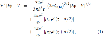
The Poisson equation associated with DDD is nonlinear,
 |

 |
Equation (
Each impurity provides a hole, so the Fermi level (EF) can be set by the electroneutrality condition 

 |


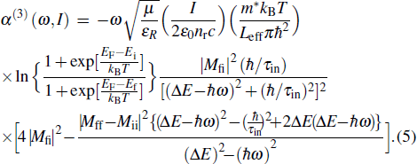
The optical properties are calculated from the obtained electronic structure. Doyeol Ahn et al.,[36] determined an expression for linear α(1) and the nonlinear α(3) intersubband optical absorption in a quantum well as follows:
 |
 |
In Ref. [31] there is a detailed analysis of the parameters involved, where Mfi represents matrix elements of the dipole moment of the final (f) and initial (i) associated states. In this case m* represents the mass of heavy holes, τin is the intersubband relaxation time. For this calculation we use τin = 0.28 ps.[37,38]
In the low temperatures limit, the obtained relative linear absorption coefficient with respect to a reference coefficient 
 |
 |
 |
In an analogous way to the absorption coefficient, we determine in the limit of low temperatures the relative term of the change of the refractive index with respect to an isolated well in the transition 1–0,
 |
The changes of the absorption coefficient and refractive index are measured with the energy difference (ΔE) and the magnetic moment (Mfi), and these parameters are functions of the distance between layers.
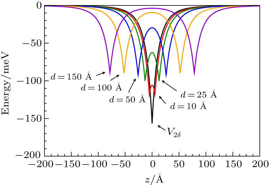
The starting parameters for p-type double delta-doped quantum wells are mhh = 0.52m0, mlh = 0.082m0, εr = 12.5, where m0 is the free electron mass. In Fig.
The solution to the Schrödinger equation is performed to determine the charge distribution across p-type doped ionized layers, according to the two-dimensional doping profile. For the doped system, the donor concentration is set to ρ2D = 1 × 1013 cm−2. The corresponding calculated potential profile, energy levels, and wave functions for the p-type DDD GaAs are depicted in Figs.
The electronic structure of our system concurs qualitatively with that reported in previous works for distances greater than 100 Å.[32,33,35] At distances below 100 Å the electronic structure is significantly different due to the physical conditions imposed in expression (
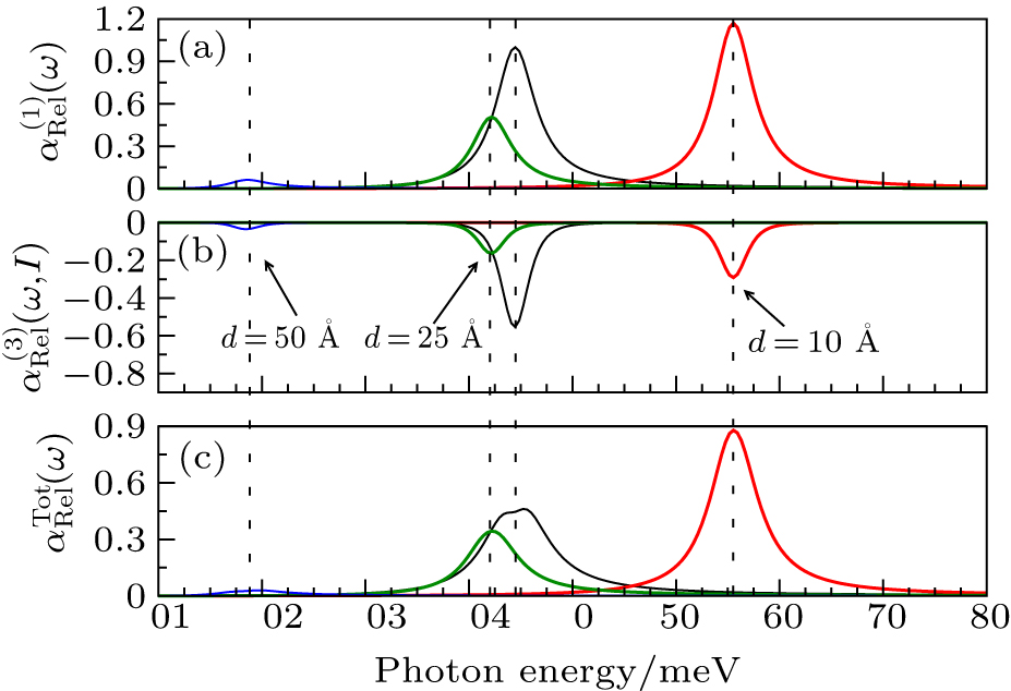
In expressions (
Figure
Our results are consistent with the absorption reported by other authors, where they performed calculations of absorption coefficient in n-type GaAs under external effects such as pressure, electric and magnetic fields,[30,40,42,43] in which they calculated the optical absorption in double doped delta systems with separation distances between layers greater than 100 Å so that the interlayer distance effects are not very important.
With the same parameters used in the absorption coefficient, the refractive index change is determined. Figure
 | Fig. 4. (a) linear, (b) non-linear and (c) total relative refractive index change as a function of the photon energy. In this figure, was used the same parameters in Fig. |
It can be observed that the distance changes between layers have a greater influence on the linear terms. This can be seen more clearly when comparing Figs.
We have theoretically studied the influence of interlayer distance on the relative linear and nonlinear absorption coefficients, besides the relative refractive index change for p-type DDD quantum wells in GaAs. In the framework of the TF approach, we calculate the electronic structure for heavy and light holes. For this system, the superposition principle is not valid at all because their Poisson equation is nonlinear. The absorption coefficient for hh has a red shift of the peak position and a decrease in amplitude when the distance between layers increases. On the other hand, the behavior of the relative refractive index change node has a red shift as the interlayer distance increases for hh. These results reveal that the interlayer distance has an important influence on the linear terms. An enhancement of the optical properties can be achieved with the adequate separation distance between ionized layers. These results are very important for engineering of optical and electronic devices.
| [1] | |
| [2] | |
| [3] | |
| [4] | |
| [5] | |
| [6] | |
| [7] | |
| [8] | |
| [9] | |
| [10] | |
| [11] | |
| [12] | |
| [13] | |
| [14] | |
| [15] | |
| [16] | |
| [17] | |
| [18] | |
| [19] | |
| [20] | |
| [21] | |
| [22] | |
| [23] | |
| [24] | |
| [25] | |
| [26] | |
| [27] | |
| [28] | |
| [29] | |
| [30] | |
| [31] | |
| [32] | |
| [33] | |
| [34] | |
| [35] | |
| [36] | |
| [37] | |
| [38] | |
| [39] | |
| [40] | |
| [41] | |
| [42] | |
| [43] |


