Impact of proton-induced alteration of carrier lifetime on single-event transient in SiGe heterojunction bipolar transistor
Wei Jia-Nan1, †, He Chao-Hui1, Li Pei1, Li Yong-Hong1, Guo Hong-Xia2
School of Nuclear Science and Technology, Xi’an Jiaotong University, Xi’an 710049, China
State Key Laboratory of Intense Pulsed Irradiation Simulation and Effect, Northwest Institute of Nuclear Technology, Xi’an 710024, China


† Corresponding author. E-mail: weijianan93@163.com

Project supported by the National Natural Science Foundation of China (Grant Nos. 11775167, 61574171, 11575138, and 11835006).

Abstract

This paper presents an investigation into the impact of proton-induced alteration of carrier lifetime on the single-event transient (SET) caused by heavy ions in silicon–germanium heterojunction bipolar transistor (SiGe HBT). The ion-induced current transients and integrated charge collections under different proton fluences are obtained based on technology computer-aided design (TCAD) simulation. The results indicate that the impact of carrier lifetime alteration is determined by the dominating charge collection mechanism at the ion incident position and only the long-time diffusion process is affected. With a proton fluence of 5×1013 cm−2, almost no change is found in the transient feature, and the charge collection of events happened in the region enclosed by deep trench isolation (DTI), where prompt funneling collection is the dominating mechanism. Meanwhile, for the events happening outside DTI where diffusion dominates the collection process, the peak value and the duration of the ion-induced current transient both decrease with increasing proton fluence, leading to a great decrease in charge collection.

1. Introduction

The electronics in spacecrafts that are routinely exposed to both extreme fluctuations in temperature and energetic particles in space may employ silicon–germanium heterojunction bipolar transistors (SiGe HBT) because of their superior low-temperature performance and built-in multi-Mrad (SiO2) total ionizing dose (TID) tolerance without intentional hardening design.[16] However, bulk SiGe HBTs are susceptible to single-event effects (SEEs), which has been proved to be their only obvious weakness for space applications, due to the existence of the large-area collector–substrate (C–S) junction.[7,8] Moreover, existing publications indicate that the sensitive area of SiGe HBTs to SEEs is not just confined in the active region (emitter/base/collector stack). The charges generated in the events many micrometers away from the active region can also be collected through a diffusion process, making the development of the model for on-orbit event rate calculation more complicated.[9,10]

In the space radiation environment, energetic particles can cause several radiation effects in semiconductor devices, including SEEs, TID, and displacement effects, at the same time. The interaction of these effects may lead to unexpected radiation responses of the devices.[1114] For SiGe HBTs, displacement defects caused by protons in the Van Allen belt and solar galactic cosmic rays can act as effective trapping and recombination centers that can reduce the minority carrier lifetime so that less minority carriers injected from the emitter can cross the base region and reach the collector junction, leading to the degradation of the transistor current gain.[15] However, it is also worth noting that the displacement defects induced by space radiation sources usually distribute uniformly in the whole device. The minority carrier lifetime is also altered in other parts of the device, such as the lightly doped substrate, which is confirmed to be a crucial feature dominating the single-event charge collection of bulk SiGe HBTs. Therefore, the transport of the charges generated in a single event may also be impacted. This may cause changes in the total charge collection, which is the main metric related to single-event upsets (SEU) in SiGe circuits. It has been confirmed that a low-temperature, grown GaAs buffer layer in GaAs HIGFET, which provides a region of high recombination and shortens the minority carrier lifetime, can significantly reduce the transient charge collection caused by the α particle.[16] However, no related publication about SiGe HBT is currently available.

In this work, the impact of proton-induced alteration of minority carrier lifetime on heavy ion-induced current transients and charge collection in SiGe HBT is investigated using technology computer-aided design (TCAD) tools. The results indicate that the charge collection of events free from deep trench isolation (DTI) is more sensitive to the alteration of minority carrier lifetime than that with DTI, especially in the heavily doped reach-through region used for substrate contact, where a decrease of 94% can be found with a proton fluence of 5×1013 cm−2.

2. Simulation details
2.1. Device structure

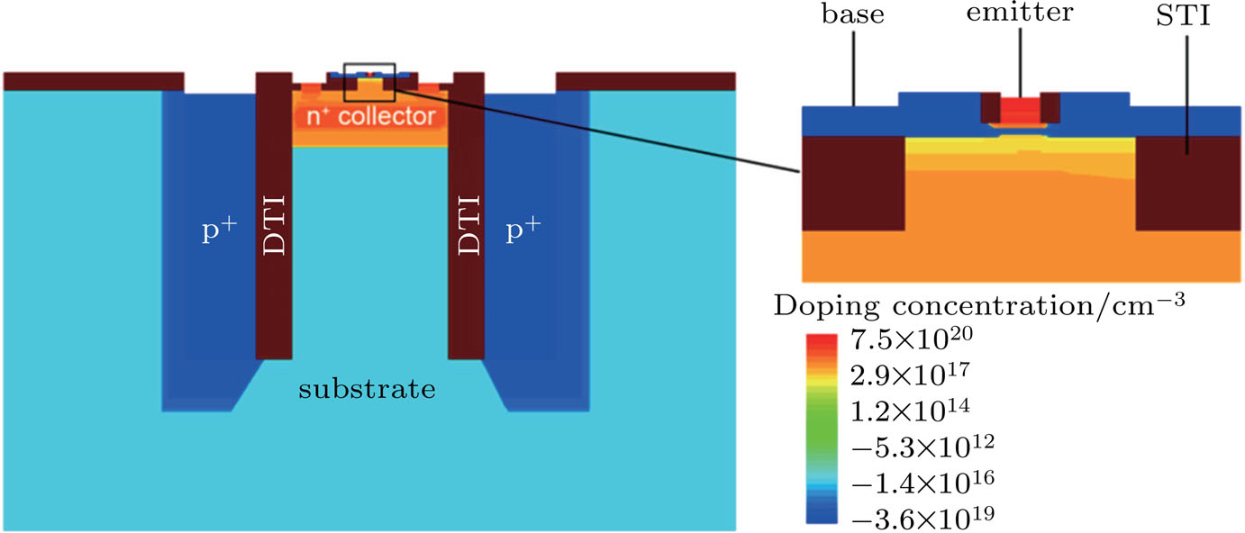
The prototype device used to build the simulation model is the IBM 8HP SiGe HBT. Figure 1 shows the two-dimensional (2D) cross section obtained from cuts made through the center of the three-dimensional (3D) device structure. The device has an npnn+ structure with a lightly doped p-type substrate. The buried n+ layer is used to reduce the collector resistance. The emitter area is . The deep trench used in DTI is wide and deep, and on top of it sits the shallow trench isolation and the intrinsic device. The area enclosed by the trench is . The p+ reach-through outside DTI is for top contact of the substrate. More details of the device can be found in Refs. [17] and [18]. The physical models considered in this work include Phillips unified mobility, Shockley–Read–Hall recombination, Auger recombination, velocity saturation, and bandgap narrowing. Figure 2 shows the Gummel characteristic obtained by TCAD simulation and tests. The simulated base and collector current fits well with the test results measured by a Keithley 4200 within a reasonable range of errors.

Fig. 1. TCAD cross section along the center line of IBM 8HP SiGe HBT.
Fig. 2. Gummel characteristic obtained by simulation and tests.
2.2. Simulation of proton-induced carrier lifetime alteration

Displacement defects are introduced into the device through collisions of the incident protons with the silicon nucleus and by collisions of the recoil primary silicon atom with near atoms. These defects can act as effective trapping and recombination centers of the carriers. As a result, some basic electric properties of semiconductors, such as the minority carrier lifetime, the majority carrier density, and the carrier mobility, will be altered. The minority carrier lifetime has been proved to be the most sensitive parameter to displacement damage, while the majority carrier density and carrier mobility remain stable with a neutron fluence up to 5×1013 cm−2.[19,20] Therefore, changes in the minority carrier lifetime are usually used to mimic displacement damage in the device. The quantitative relationship between the minority carrier lifetime and displacement damage is usually given involving neutron fluence as follows: where τ is the minority carrier lifetime before neutron irradiation, is the minority carrier lifetime after neutron irradiation, is the coefficient of neutron-induced alteration of the minority carrier lifetime (for neutrons with energy above 10 keV, ),[21] and is the neutron fluence. According to the national military standards for testing neutron radiation effects on military electronic devices, the displacement damage in semiconductor materials induced by neutrons with a spectral energy distribution is characterized by 1 MeV neutrons with an equivalent fluence. For silicon devices, the equivalent 1 MeV neutron fluence is defined as where is the equivalent 1 MeV neutron fluence, is the fluence of the neutron group with energy E, D(E) is the damage factor (Kerma factor) of neutrons with energy E in silicon, and D(1 MeV) is the damage factor of 1 MeV neutrons in silicon. Thus, in Eq. (1) actually refers to the equivalent fluence of 1 MeV neutrons. When it comes to protons, it is necessary to know the equivalent proton fluence to . Since the displacement damage is generated during atomic processes due to the nonionization energy loss (NIEL) of the incident particle, the equivalence can be made by comparing the NIELs of neutrons and protons with different energies in silicon.[22] Therefore, equation (1) can be rewritten as where .

In this work, the 30 MeV proton is selected to generate the lifetime alteration. The NIEL of the 30 MeV proton in silicon calculated using Geant4 is about . The NIEL of the 1 MeV neutron in silicon is about .[23] The minority carrier lifetime of each region in the SiGe HBT recalculated with Eq. (3) is used to replace the default value in the parameter file.

Figure 3 shows the current gain (β) considering proton-induced alteration of the minority carrier lifetime using the method mentioned above. With the increase in , the minority carrier lifetime decreases monotonically, which increases the recombination rate in the base and leads to the significant degradation of β. This is consistent with the results in Refs. [14] and [15], indicating that the model we built is reasonable.

Fig. 3. Current gain of IBM 8HP considering proton-induced alteration of minority carrier lifetime.

This model can also be extrapolated to other SiGe HBT devices. For one thing, the NIEL of middle- and high-energy protons is almost equivalent to that of neutrons.[24] In the real space applications, low-energy protons are easily shielded by the spacecraft walls, and it is hard for the fluence of middle- and high-energy protons to exceed the order of 5×1013 cm−2. Furthermore, the relationship between the minority carrier lifetime and neutron or proton fluence does not involve the geometry of the target material. However, the impact of the alteration of the minority carrier lifetime on the ion-induced single-event transient (SET) may be different from device to device due to the devices’ structures, as will be shown later.

2.3. Simulation conditions

During simulation, the emitter, base, and collector are biased at 0 V, while the substrate is biased at −3 V. Under this condition, the C–S junction is reverse biased. When a heavy ion passes through the junction, the excess carriers deposited can be rapidly collected, leading to a current transient at the collector. Since the collector is usually the output terminal of SiGe HBT in ICs, the ion-induced current transient may cause disturbances in the following components. Therefore, these bias conditions replicate the most sensitive state to SEEs.[2527] Concretely, the initial voltage boundary conditions of all terminals of the SiGe HBT are set to 0 V in the electrode section of Sentaurus Device, and then these boundary conditions are ramped to the worst biasing conditions in the Solve section of the command file using the quasistationary command. Ohmic contacts are implemented through the Dirichlet boundary condition, in which the quasi Fermi potentials of majority and minority carriers are equal to the applied voltage on the electrode.[28] The outer boundaries of the device that are not contacts are treated with the ideal Neumann boundary condition and the current in the device can only flow through the contacting node. Similarly, the Neumann boundary condition is also applied to the semiconductor/insulator interfaces to avoid the current in the semiconductor from flowing into the insulator. The simulated ion strike is 209Bi with an LET of 99.8 MeV cm2 mg−1. This is the highest LET among the frequently used ions in domestic heavy ion accelerator experiments. The ion track is generated using a Gaussian waveform in which the 1/e characteristic time scale is 2 ps, the peak of the Gaussian distribution occurs at 5 ps, and the 1/e characteristic radius is . All the ions are normal incident. Due to the high LET value, a large amount of charge will be generated along the ion track so that even the charge collection of the event outside the deep trench can reach a considerable value. Figure 4 shows the ion strike positions. All the positions distribute along the center line of the device. The x-axis coordinates are , , , , , , , , , , , and from left to right. Therefore, variations in the charge collection of events inside and outside the deep trench are all studied.

Fig. 4. Diagram of the ion strike positions along the x-axis.
3. Simulation results

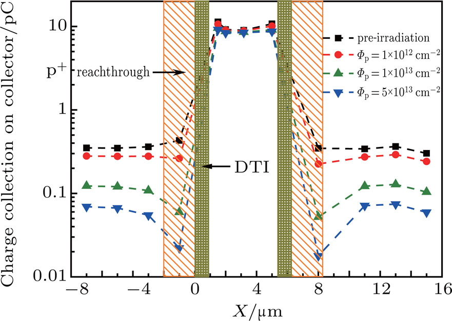
Figure 5 shows the simulation results of charge collection on the collector terminal as a function of ion incident position. The proton fluence varies from 0 to 5×1013 cm−2. It is clear that the charge collection inside the deep trench is much higher than that outside. This has also been reported in previous publications. The reason is that DTI blocks the expansion of the funnel potential and the diffusion of the ion-induced charges so that most of the charges can be collected by funneling. On the contrary, if the ion strike happens outside the deep trench, the generated charges that are free from the pre-existing electric field are collected through diffusion. Moreover, due to the blockage from the DTI, only from the bottom can the charges diffuse to the collecting node. Therefore, only a small amount of the charges can be collected. However, with the decrease in the critical charge of ICs, events outside DTI are also able to cause SEUs. A pseudorandom number sequence generator fabricated in the IBM 7HP SiGe HBT process was reported to have a critical charge of about 100 fC.[29] The minimum charge collection of the pre-irradiation device in this work is more than 300 fC.

Fig. 5. Simulation results of charge collection as a function of ion incident position.

The impact of proton-induced carrier lifetime alteration on the charge collection inside and outside DTI also differs a lot. The lifetime alteration has almost no impact on the charge collection of events happening inside the deep trench, but it does reduce the charge collection of events happening outside the trench by a large extent. With increasing , the charge collection decreases monotonically. When reaches 5×1013 cm−2, the charge collection of all events happening in the lightly doped substrate decreases by about 80% and is below 100 fC. For the events in the p+ reach-through, some distinctions in the rate of decreasing charge collection can be found. As can be seen from Fig. 5, when , the charge collection of events in the p+ region only slightly decreases, just for the events in the lightly doped substrate. Meanwhile, at higher fluences, the charge collection in the p+ region decreases much faster than at other positions. When reaches 5×1013 cm−2, the decrease can even exceed 94%.

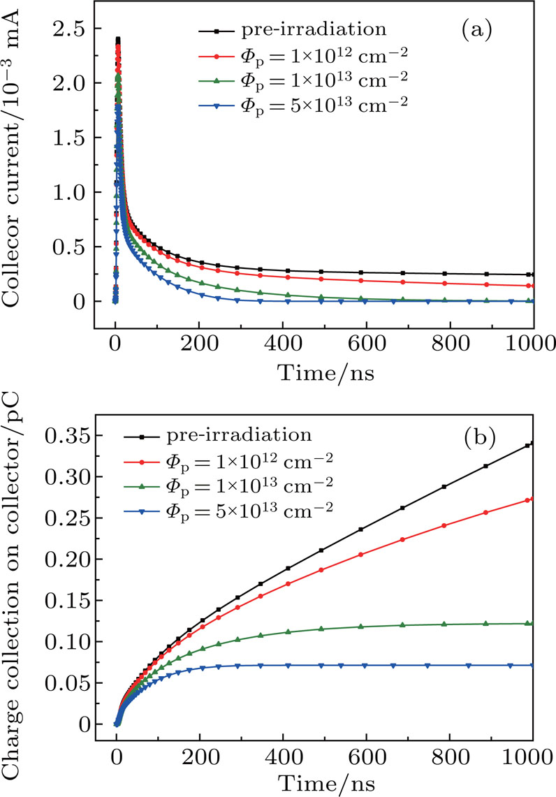
Figure 6 shows the current transients and integrated charge collections on the collector terminal at (center of the device) under various proton fluences. According to the timescale of different collection mechanisms, the current transient can be generally divided into two parts, as shown in Fig. 6(a). The prompt high-current peak before 1 ns is mainly due to the funneling collection. The transients at different proton fluences overlap within this part, indicating that the charge collection is not affected by the carrier lifetime alteration. The other part, which results from the delayed charge collection by diffusion, features a low-magnitude long-timescale current tail. In this part, slight shifts left at the end of the tail with increasing proton fluence can be found, which can lead to the decrease in integrated charge collection. However, this decrease is much smaller compared with the total charge collection, and thus the saturation value of the integrated charge collection in Fig. 6(b) does not show significant change as the proton fluence increases.

Fig. 6. Ion-induced (a) current transients and (b) charge collections at .

Figure 7 shows the current transients and integrated charge collections on the collector terminal at under various proton fluences. At this position, the generated charges are collected only through diffusion so that the peak of the current transient is much lower than that in Fig. 6(a). However, the duration of the transient is much longer. The transient can last more than (upper limit of the simulation time in this work) if the minority carrier lifetime is not altered. Correspondingly, the charge collection keeps increasing before and does not show a trend to saturation. With the increase in proton fluence, the peak value of the current transient decreases significantly and so does the transient duration. When the proton fluence reaches 5×1013 cm−2, the peak value of the current transient decreases from to , and the duration decreases to 300 ns. As a result, the time needed by the charge collection to reach saturation and the total charge collection both decrease with increasing proton fluence.

Fig. 7. Ion-induced (a) current transients and (b) charge collections at .
4. Discussion

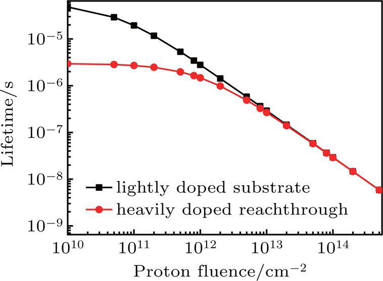
As depicted above, the proton-induced decrease in minority carrier lifetime only reduces the charge collection that is due to the long-time diffusion, and has no impact on the charge collection that is due to funneling. This indicates that the impact of the minority carrier lifetime may be related to the timescale of the collection mechanism. Figure 8 shows the maximum minority carrier lifetimes in the lightly doped substrate and heavily doped reach-through as a function of . When , the minority carrier lifetimes in the two regions both decrease to about 60 ns. Since the duration of the diffusion process can exceed , this decrease in minority carrier lifetime will lead to a great decrease in the charge collection of events outside the deep trench. Meanwhile, for the events happening inside the deep trench, the charge collection is dominated by funneling. According to Fig. 6(a), this process finishes in 1 ns, and thus the reduced minority carrier lifetime has little impact on the total charge collection.

Fig. 8. Maximum minority carrier lifetime as a function of proton fluence.

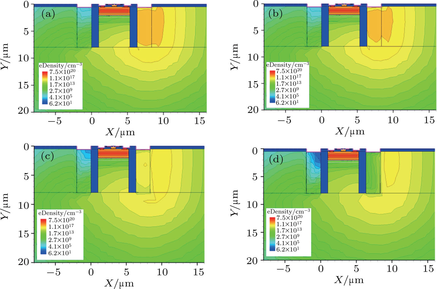
For the events happening in the p+ reach-through, the mechanism is more complicated. Since the doping concentration in the p+ reach-through is several orders of magnitude higher than that in the substrate, the ion-induced electrons and holes have to undergo a stronger initial recombination there. Only the electrons that escape from this recombination and reach the lightly doped substrate through radial diffusion can contribute to the charge collection on the collector terminal. With the increase in proton fluence, more recombination centers are generated in the p+ region, which in turn promotes the initial recombination. As a result, the charge collection of events happening in the p+ reach-through has a more significant decrease with increasing proton fluence. In addition, the pre-irradiation minority carrier lifetime in the p+ reach-through is relatively short, and thus a significant amount of displacement damage is needed to affect it.[20] As shown in Fig. 8, the maximum minority carrier lifetime in the p+ reach-through is only slightly reduced when , while more significant decrease can be found after 1×1013 cm−2. Figure 9 shows the electron density at 1.2 ns when the ion strikes at . It is clear that when (see Fig. 9(b)), the electron density is very close to that in the pre-irradiation device (see Fig. 9(a)). When reaches 1×1013 cm−2, the electron density around the track becomes much lower, especially in the p+ reach-through (see Fig. 9(c)). When reaches 5×1013 cm−2, the electron density in the p+ reach-through decreases to a magnitude comparable to the density deep in the substrate (see Fig. 9(d)). This sharp decrease confirms the enhanced recombination in the p+ region. Consequently, fewer electrons are able to diffuse into the lightly doped region. This explains the sharp decrease of the charge collection of events in the p+ reach-through at high-proton fluences, as shown in Fig. 5.

Fig. 9. Electron density at 1.2 ns when the ion strikes at with (a) , (b) , (c) , and (d) .
5. Conclusion

In this work, the impact of proton-induced alteration of the minority carrier lifetime on the ion-induced current transient and charge collection in the SiGe HBT with DTI is investigated using TCAD tools. The widely used equation to determine the neutron-induced alteration of the minority carrier lifetime in silicon is extended for use with the to proton by normalizing to the energy going into the atomic process. Simulation results show that the impact of proton-induced alteration of carrier lifetime on the current transient and the integrated charge collection is position-dependent and is closely related to the timescale of the dominating charge collection mechanism. Only the long-time collection process is significantly affected. For the events inside the deep trench, the charge collection is dominated by prompt funneling and is little affected. Meanwhile, for the events outside the deep trench, the charge is collected only by diffusion, and thus a large amount of charges recombine during transport, leading to a great decrease in the total charge collection. Particularly, the decrease is more remarkable in the p+ reach-through due to the enhanced initial recombination of ion-induced charges before they diffuse into the lightly doped substrate.

Reference
[1] Sutton A K Haugerud B M Lu Y Kuo W L Cressler J D Marshall P W Reed R A Rieh J S Freeman G Ahlgren D 2004 IEEE Trans. Nucl. 51 3736
[2] Cressler J D 2013 IEEE Trans. Nucl. Sci. 60 1992
[3] Marshall P W Carts M A Campbell A McMorrow D Buchner S Stewart R Randall B Gilbert B Reed R A 2000 IEEE Trans. Nucl. Sci. 47 2669
[4] Cressler J D Hamilton M C Mullinax G S Li Y 2000 IEEE Trans. Nucl. Sci. 47 2515
[5] Cressler J D 2005 P. IEEE 93 1559
[6] Krithivasan R Lu Y Cressler J D Rieh J S Kater M H Ahlgren D Freeman G 2006 IEEE Electron Device Lett. 27 567
[7] Comeau J P Sutton A K Haugerud B M Cressler J D Kuo W L Marshall P W Reed R A Karroy A Rogeret V A 2004 IEEE Trans. Nucl. Sci. 51 3743
[8] Montes E J Reed R A Pellish J A Alles M L Schrimpf R D Weller R A Varadharajaperumal M Niu G Sutton A K Diestelhorst R 2008 IEEE Trans. Nucl. Sci. 55 1581
[9] Pellish J A Reed R A Schrimpf R D Alles M L Varadharajaperumal M Niu G Sutton A K Diestelhorst R M Espinel G Krithivasan R Comeau J P Cressler J D Vizkelethy G Marshall P W Weller R A Mendenhall M H Montes E J 2006 IEEE Trans. Nucl. Sci. 53 3298
[10] Marshall P Carts M Currie S Reed R Randall B Fritz K Kennedy K Berg M Krithivasan R Siedleck C 2005 IEEE Trans. Nucl. Sci. 52 2446
[11] Zheng Q Cui J Lu W Guo H Liu J Yu X Wei Y Wang L Liu J He C 2018 IEEE Trans. Nucl. Sci. 65 1920
[12] Wei J N Guo H X Zhang F Q Luo Y H Ding L L Pan X Y Zhang Y Liu Y H 2017 Chin. Phys. 26 096102
[13] Pan X Y Guo H X Luo Y H Zhang F Q Ding L L Wei J N Zhao W 2017 Chin. Phys. 26 018501
[14] Wang C Bai X Wei C Yang S Liu Y Jin X Ding L 2015 Nucl. Instrum. Meth. 796 108
[15] Petrosyants K O Kozhukhov M V 2016 IEEE Trans. Nucl. Sci. 63 2016
[16] McMorrow D Weatherford T R Curtice W R Knudson A R Buchnerf S Melinger J S Tran L H Campbell A B 1995 IEEE Trans. Nucl. Sci. 42 1837
[17] Varadharajaperumal M Niu G Krithivasan R Cressler J D Reed R A Marshall P W Vizkelethy G Dodd P E Joseph A J 2003 IEEE Trans. Nucl. Sci. 50 2191
[18] Niu G Yang H Varadharajaperumal M Shi Y Cressler J D Krithivasan R Marshall P W Reed R 2006 IEEE Trans. Nucl. Sci. 52 2153
[19] Srour J R Marshall C J Marshall P W 2003 IEEE Trans. Nucl. Sci. 50 653
[20] Srour J R Palko J W 2013 IEEE Trans. Nucl. Sci. 60 1740
[21] Srour J R Chen S C Othmer S Hartmann R A 1979 IEEE Trans. Nucl. Sci. 26 4783
[22] Messenger G C 1992 IEEE Trans. Nucl. Sci. 39 468
[23] Srour J R Vendura G J Lo D H Toporow C M C Dooley M Nakano R P King E E 1998 IEEE Trans. Nucl. Sci. 45 2624
[24] Wang Y et al. 2013 High Power Laser Part. Beams 25 1803
[25] Chu P Hansen D L Doyle B L Jobe K Lopez R A Shoga M Walsh D S 2006 IEEE Trans. Nucl. Sci. 53 1574
[26] Sun Y Fu J Wang Y Zhou W Liu Z Li X Shi Y 2016 Microelectron. Reliab. 65 41
[27] Krithivasan R Niu G Cressler J D Currie S M 2003 IEEE Trans. Nucl. Sci. 50 2126
[28] Fu Y Li Z Ng W T Johnny K O Sin 2014 Integrated Power Devices and TCAD Simulation 1 Boca Raton CRC Press 91
[29] Reed R A Marshall P W Pickel J C Carts M A Fodness B Niu G Fritz K Vizkelethy G Dodd P E Irwin T 2003 IEEE Trans. Nucl. Sci. 50 2184