Analysis of displacement damage effects on bipolar transistors irradiated by spallation neutrons
Liu Yan1, 2, Chen Wei2, †, He Chaohui1, Su Chunlei2, Wang Chenhui2, Jin Xiaoming2, Li Junlin2, Xue Yuanyuan2
School of Nuclear Science and Technology, Xi’an Jiaotong University, Xi’an 710049, China
State Key Laboratory of Intense Pulsed Radiation Simulation and Effect (Northwest Institute of Nuclear Technology), Xi’an 710024, China


† Corresponding author. E-mail: chenwei@nint.ac.cn

Abstract

Displacement damage induced by neutron irradiation in China Spallation Neutron Source (CSNS) is studied on bipolar transistors with lateral PNP, substrate PNP, and vertical NPN configurations, respectively. Comparison of the effects on different type transistors is conducted based on displacement damage factor, and the differences are analyzed through minority carrier lifetime calculation and structure analysis. The influence of CSNS neutrons irradiation on the lateral PNP transistors is analyzed by the gate-controlled method, including the oxide charge accumulation, surface recombine velocity, and minority carrier lifetime. The results indicate that the total ionizing dose in CSNS neutron radiation environment is negligible in this study. The displacement damage factors based on 1-MeV equivalent neutron flux of different transistors are consistent between Xi’an pulse reactor (XAPR) and CSNS.

1. Introduction

Bipolar circuits are widely used in satellites and spacecraft due to their excellent current drive capability, linearity, and matching characteristics.[1] However, various particles and rays in the space environment can cause serious degradation of their performance.[2] Displacement damage is one of the important factors leading to the degradation of bipolar transistor performance. Many investigations have been carried out on the displacement damage effect of bipolar transistors,[3,4] and some people have even used the gain degradation models to measure the particle fluence.[5]

Neutrons, protons, and electrons can cause displacement damage in semiconductor materials.[2] However, protons and electrons may have a synergistic effect due to the charge carried, and the charge accumulation at the surface of the semiconductor devices may affect the displacement damage.[69] Therefore, neutrons are suitable for displacement damage study. With the operation of China Spallation Neutron Source (CSNS), it can provide a wider neutron energy spectrum, a higher neutron portion, and a lower ionizing dose.[10,11] It is of great significance to use the CSNS to study the displacement damage effect. In this paper, the differences between the damage effects of the transistors caused by CSNS and Xi’an pulse reactor (XAPR) were analyzed by using the gate-controlled lateral PNP (LPNP) transistors, the vertical NPN (VNPN) transistors, and the substrate PNP (SPNP) transistors. The degradation of minority lifetime, oxide charge accumulation, and surface recombine velocity parameters were analyzed by charge separation method, and the effects were analyzed by calculation.

2. Experimental details

The transistors were specially designed and manufactured by the State Key Laboratory of Analog Integrated Circuit, Chongqing, China using the 8- process. Three kinds of bipolar transistors are different in the structure, and other parameters are fixed. The doping concentration of the epitaxial layer is 1.5×1015 cm−3, the oxide layer thickness is , the emitter doping concentration is 1.0×1019 cm−3, the junction depth is , and the base region doping concentration of the NPN transistors is 8.0×1017 cm−3. The typical layouts and cross-sectional views of the transistors are illustrated in Section 4, and their main parameters are summarized in Table 1.

Table 1.

Main parameters of the transistors.

.

Reactor neutrons irradiation on the transistors was performed using a training, research, isotopes, general atomics (TRIGA) nuclear reactor, i.e., Xi’an pulse reactor. The XAPR was operated with the power of 100 kW, the 1-MeV equivalent neutron flux rate was 5.8×109 cm−2 s−1, and the neutron/gamma ray ratio (n/γ ratio) was 7.7×109 cm−2 rad(Si)−1. The neutron energy was distributed between 10 keV and 10 MeV, and the mean value of neutron energy was about 1 MeV (Fig. 1).[12] The accuracy of neutron fluence measurement was within ±7.5%. In this paper, the reactor neutron fluence is given as the 1-MeV equivalent fluence.

Fig. 1. Experimental neutron energy spectrum of XAPR.

The spallation neutrons irradiation on the transistors was performed at CSNS with the 20-kW operating power, and the proton beam pulses were accelerated to 1.6 GeV at 25-Hz repetition rate, striking a solid lead (Pb) target to produce spallation neutrons.[10] The neutron flux rate is 2.72×106 cm−2 s−1 under 20-kW operating power in this study. It is necessary and convenient to convert neutron counts into 1-MeV neutron equivalent fluence for displacement damage study. Based on the American Society for Testing and Materials (ASTM) E722 standard, a 1-MeV neutron equivalent fluence conversion coefficient of energy above 0.01 MeV is calculated according to the CSNS neutron spectra (Fig. 2). The conversion coefficient is shown in Fig. 3. The 1-MeV neutron equivalent converting calculations make the effects induced by two neutron environments comparable.

Fig. 2. Theoretical neutron energy spectrum of CSNS.
Fig. 3. The 1-MeV neutron equivalent conversion coefficient of CSNS.

During irradiation, all the pins were shorted to the ground, and after exposures, the gain parameters of the transistors were measured with an HP4156A semiconductor parameter analyzer. The measuring method was as follows: for the PNP transistors, the collector was grounded, the emitter was maintained at 2 V, and the base voltage was swept from 2 V to 1 V; for the NPN transistors, the emitter was grounded, the collector was maintained at 2 V, and the base voltage was swept from 0 V to 1 V.

3. Experimental results

Current gain is one of the most important electrical parameters for bipolar transistors. The current gain degradation induced by displacement damage is well described by Messenger–Spratt equation[13]

where hFE is the current gain of the transistors, which equals IC divided by IB. is the energy-dependent displacement damage factor, and Φis the incident neutron fluence. According to the linear relationship of the equation, we can calculate the damage factor of the gain under the same collector current for comparison. For PNP transistors, IC was fixed at 2×10⁻⁵ A, and 6×10⁻⁴ A for NPN transistors’ IC.

The transistors are irradiated by reactor neutrons up to 2.3×1013 cm−2, and spallation neutrons up to 4.97×1011 cm−2 (VNPN up to 7.0×1011 cm−2). The data are measured in situ at regular intervals, respectively. The neutron fluence described here is 1-MeV neutron equivalent fluence.

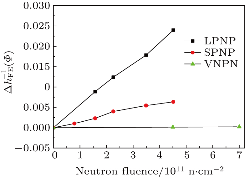
The ( ) versus Φcurves for the lateral PNP transistor, substrate PNP transistor, and vertical NPN transistor irradiated by reactor neutrons and spallation neutrons are illustrated in Figs. 4 and 5. The damage factors for the three types of transistors are listed in Table 2.

Fig. 4. ( ) versus neutron fluence Φfor LPNP, SPNP, and VNPN bipolar transistors irradiated by XAPR.
Fig. 5. ( ) versus neutron fluence Φfor LPNP, SPNP, and VNPN bipolar transistors irradiated by CSNS.
Table 2.

Displacement damage factors of the transistors.

.

The data show that the lateral PNP transistor is most sensitive, the substrate transistor is the second, and the vertical NPN transistor is the least sensitive in this study. From the comparison of damage factors in two environments, the displacement damages induced by CSNS neutrons are slightly lower than XAPR. Figure 2 shows the neutron spectrum generated by CSNS. 14% of the neutrons are less than 0.1 MeV, 40% are from 0.1 MeV to 1 MeV, 41% are from 1 MeV to 20 MeV, and 5% are above 20 MeV. The 1-MeV neutron equivalent conversion coefficient of CSNS is conducted according to ASTM E722. But the ASTM standard only covers neutrons with energies below 20 MeV. In this study, the silicon displacement damage kerma factor of neutrons above 20 MeV is uniformly set to 182.87 MeV mb, which may cause the difference of the damage factors. However, in the range of measurement uncertainty, we can still conclude that the results are consistent. The results also indicate the non-ionizing energy loss (NIEL) methodology is suitable to normalize the displacement damage induced by neutrons with different energy spectra.[14]

4. Discussion
4.1. Analysis of effect differences

As mentioned in [15], the reciprocal gain is given by

The gain is determined by five current components from the following parts: bulk base recombination IRB, recombination-generation in B–E depletion layer IRG, B–E minority carrier reverse diffusion ID, BE surface leakage IS, and B–C reverse leakage ICBO. Considering the displacement damage, the bulk base recombination current IRB plays the most important role of these components, which is given by
where q is electronic charge, Ae is emitter area, Wb is base width, nbo is thermal equilibrium minority carrier concentration in the base, is minority carrier lifetime in the base, and k is Boltzmann’s constant. It can be seen from Eq. (3) that the bulk base recombination current is mainly affected by the width and the minority carrier lifetime of the base. In this study, the base width of the three transistors are: LPNP , SPNP , and VNPN . Therefore, minority carrier lifetime dominates the displacement damage effect. The minority carriers in NPN transistor base region are electrons, while those in PNP transistor base region are holes. We can calculate the individual minority carrier lifetime using empirical equations[16]

Base on the process parameters of the transistors introduced in Section 2, it can be calculated that the , under initial conditions. Obviously, the minority carrier lifetime of PNP transistors is much longer than that of NPN transistors. For bipolar devices, minority carrier lifetime shortening is the most important effect. The longer the initial lifetime is, the more sensitive the devices are.[17] The PNP transistors are more vulnerable to displacement damage than NPN transistors. In addition, the lateral PNP transistor has the largest emitter perimeter ( ) in this study, the substrate transistor is the second ( ), and the vertical NPN transistor is the least ( ). The emitter perimeter values also lead to the discrepancy on different transistors. The bulk base recombination current IRB could be also written as:

where q is electronic charge, and R is bulk recombination rate. V is volume of the bulk recombination, which is proportional to emitter perimeter and base width. Obviously, the LPNP has a larger bulk base recombination current than the substrate PNP and vertical NPN transistors, leading to more severe degradation after neutron irradiation.

On the other hand, the parasitic structure inside the transistors may also affect the displacement damage effect. The cross-sectional view and parasitic structure schematic diagram of the lateral PNP transistor are illustrated in Fig. 6.

Fig. 6. Cross-sectional view and parasitic structure schematic diagram of the lateral PNP transistor: (a) cross-sectional view of the lateral PNP transistor, (b) two parasitic transistor in LPNP, and (c) reverse biased collector.

The parasitic transistor structures in LPNP are composed of E (emitter)–B (base)–S (substrate) and C (collector)–B (base)–S (substrate), respectively. In the test conditions of this study, the collector is grounded and the emitter is connected to high potential, thus the C–B–S parasitic structure would not affect the gain parameters of LPNP. But the influence of E–B–S parasitic transistor could not be ignored,[18] and it will significantly reduce the gain of LPNP, which will be more significant when it is affected by displacement damage. Only holes injected from the side of the emitter contribute to the gain of LPNP, and holes injected at the bottom of the emitter contribute to the gain of the parasitic PNP transistor. The base current measured in this paper is indeed the superposition of the base currents of E–B–C and E–B–S transistors. Under the combined action of two transistors, the excess base current after neutron irradiation could increase significantly.

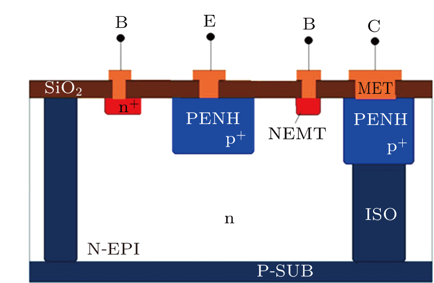
The cross-sectional view of the substrate PNP transistor is illustrated in Fig. 7. The collector of the substrate PNP transistor is the common substrate of the whole circuit, and there is no parasitic structure that could affect the SPNP parameter.

Fig. 7. Cross-sectional view of the substrate PNP transistor.

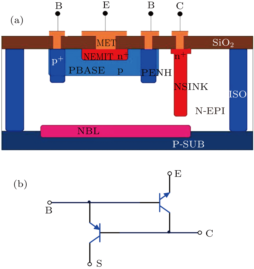
Figure 8 shows the cross-sectional view and parasitic structure schematic diagram of the vertical NPN transistor. The PNP transistor is a parasitic structure, which is composed of B–C–S. In the NPN test conditions of this study, the emitter is grounded and the collector is connected to high potential, thus the parasitic PNP transistor is in the off state and would not affect the gain of the NPN transistor.

Fig. 8. Cross-sectional view and parasitic structure schematic diagram of the vertical NPN transistor: (a) cross-sectional view of the vertical NPN transistor and (b) parasitic transistor in VNPN.
4.2. Further study of radiation effects induced by CSNS using GCLPNP

The gate-controlled lateral PNP bipolar transistor (GCLPNP) can be considered as a combination of bipolar transistor and metal–oxide–semiconductor field-effect transistor (MOSFET).[19] The cross-sectional view and structure schematic diagram of the GCLPNP transistor are illustrated in Fig. 9.

Fig. 9. Cross-sectional view and structure schematic diagram of the GCLPNP transistor: (a) cross-sectional view of the GCLPNP transistor and (b) structure schematic diagram in GCLPNP transistor.

The addition of a gated electrode to the base oxide layer allows dynamic control of the carrier concentrations at the surface of the transistor. By sweeping the gate voltage, the transistor can be operated in accumulation, depletion, or inversion modes while still biased in the forward active region of operation, allowing the device to exhibit both MOSFET and bipolar junction transistor (BJT) characteristics. In the measurements, the collector and base are grounded, the emitter is maintained at 0.45 V, and the gate voltage is swept from 10 V to −50 V.

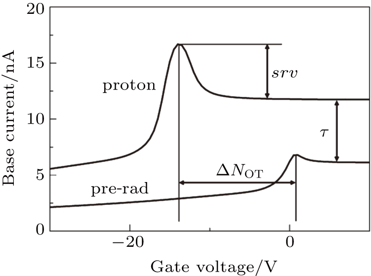
According to [18], the surface recombination velocity srv, the net increase in positively trapped charge in the oxide , and minority lifetime τ could be approximately calculated by

where q is electronic charge, pE is emitter perimeter, hE is emitter junction depth, IB is base current under cumulative condition, ni is the intrinsic carrier concentration, xB is the active base width, ND is the doping level of the base, xd is the width of the depletion region between the emitter and the base, COX is the capacitance of the oxide, is the change in the height of the base current peak, and Speak is the surface area over the active base region. In short, the change in the peak voltage position of the curve characterizes the effect of the oxide trap charge, the relative peak height characterizes the surface recombination velocity, and the overall rise of the curve characterizes the change in minority lifetime. A typical relationship of base current versus gate voltage before and after proton irradiation is shown in Fig. 10.[19] Using gate control, the effects of ionization and displacement damage for CSNS neutron irradiation can be separated and analyzed independently.

Fig. 10. Typical result of base current versus gate bias for both proton and prerad situations.

The base current response for the GCLPNP transistor is shown in Fig. 11. The pre-rad curve and those for devices exposed to different neutron fluence exhibit similar qualitative characteristics, but each data set is quite different from the others in average value of the base current under cumulative condition.

Fig. 11. Experimental base current versus gate bias on GCLPNP irradiated by different level CSNS neutrons.

The ionizing dose factors analyzed by charge separation method are listed in Table 3. Figure 12 is the experiment result of base current versus gate bias on GCLPNP irradiated by different level total ionizing doses. The GCLPNP transistors are irradiated by cobalt source gamma rays. The total ionizing dose effect causes negative drift of gate voltage, and increases with the total dose. It can be seen from Table 3 that the influence of ionizing radiation caused by different level spallation neutrons is negligible, and the surface recombination velocity and oxide trap charge even exhibit a slight decrease.

Fig. 12. Experimental base current versus gate bias on GCLPNP irradiated by different level total ionizing dose.
Table 3.

Ionizing dose factors of GCLPNP transistors irradiated by CSNS neutrons.

.

Except for the extra gate, the GCLPNP and LPNP have the same process parameters. According to a series of process parameters introduced in Section 2, the minority lifetime of GCLPNP is calculated. Equation (10) equals

The minority carrier lifetime before and after CSNS neutron irradiation is calculated, as listed in Table 4. By qualitatively comparing with the pre-rad calculation result of empirical Eq. (5), the calculation result of Eq. (10) could be considered to be reliable.

Table 4.

Minority lifetime of GCLPNP transistors irradiated by CSNS neutrons.

.

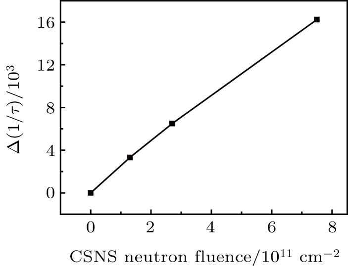
The minority carrier lifetime degradation for the GCLPNP transistor is shown in Fig. 13. The change in the reciprocal of carrier lifetime is linear with the neutron fluence, which is consistent with the literature.[20]

Fig. 13. versus CSNS neutron fluence on GCLPNP transistor.
5. Conclusion

Displacement damage of LPNP, SPNP, and VNPN transistors induced by reactor neutrons and spallation neutrons is consistent according the NIEL methodology. Besides the base width and emitter area, the parasitic structure inside the transistor circuit also plays an important role affecting the displacement damage effect. Using a gate-controlled LPNP BJT as a test device, the effects of ionizing dose and displacement damage can be examined, respectively. It is shown that minority lifetime degradation dominates the CSNS neutron radiation response, while the change of oxide traps and surface recombination velocity are negligible. This gate biasing technique provides a convenient method to analyze the details of ionization and displacement damage in irradiated BJTs.

Acknowledgment

The authors are grateful to Jingyu Tang and Zhixin Tan of Institute of High Energy Physics, Chinese Academy of Sciences for their useful support of this work.

Reference
[1] Johnston A H Rax B G 2006 IEEE Trans. Nucl. Sci. 53 1779
[2] Raymond J Peterson E 1987 IEEE Trans. Nucl. Sci. 34 1622 https://doi.org/CDSTIC.IEL.iel2007_1.23.4337426.04337526
[3] Sparks M H 1989 IEEE Trans. Nucl. Sci. 36 1904
[4] Barnaby H J 2017 IEEE Trans. Nucl. Sci. 64 149
[5] ASTM E 1855 2007, Annual Book of ASTM Standards.
[6] Li X J Liu C M 2013 IEEE Trans. Nucl. Sci. 60 3924
[7] Liu C M Li X J 2015 Radiat. Phys. Chem. 111 36
[8] Li X J Liu C M 2015 IEEE Trans. Nucl. Sci. 62 1375
[9] Li X J Geng H B Liu C M 2010 IEEE Trans. Nucl. Sci. 57 831
[10] Fu S N 2013 4th International Particle Accelerator Conference May 12–17, 2013 Shanghai, China
[11] Jing H T 2010 NuclInstrum. Methods. Phys Res. 621 91
[12] Liu S H Jiang X B 2006 Second Asian Oceanic Congress for Radiat. Prot. October 9–13, 2006 Beijing, China
[13] Conrad E E 1994 IEEE Trans. Nucl. Sci. 41 2648
[14] Liu C M Li X J 2012 Nucl. Instrum. Methods Phys. Res. 677 61
[15] John B Smyth J 1977 IEEE Trans. Nucl. Sci. 24 2093
[16] Taur Y 2009 Fundamentals Of Modern VLSI Devices 2 New York Cambridge University Press 62
[17] Srour J R 2013 IEEE Trans. Nucl. Sci. 60 1740
[18] Zhu Z Y 2001 Semicond. Integr. Circuits Beijing Tsinghua University Press 28 in Chinese
[19] Ball D R Schrimpf R D Barnaby H J 2002 IEEE Trans. Nucl. Sci. 49 3185
[20] Srour J R 2006 IEEE Trans. Nucl. Sci. 53 3610