School of Electronic and Information Engineering, Hebei University of Technology, Tianjin 300401, China
† Corresponding author. E-mail:
zhaohd@hebut.edu.cn
1. IntroductionGaN high-electron-mobility transistors (HEMTs) are a promising candidate for high-frequency applications due to their excellent material properties.[1–3] To operate the device at a high frequency, the gate length (LG) needs to be shortened. However, when the aspect ratio (LG/d, where d is the gate-to-channel distance) downscales below 15,[4, 5] short-channel effects (SCEs), such as shift of threshold-voltage, high sub-threshold swings, and increased output conductance, will become evident, which limits further improvement in the device performance. Under a poor aspect ratio, the basic technical route to the suppressing of the SCEs is to improve the control of the gate-to-channel by enhancing two-dimensional electron gas (2DEG) confinement.[6–11]
Wurtzite (WZ) BGaN ternary alloys (hereafter BGaN), as an emerging member of the III-nitride family, have introduced many innovations in optical and electronic device applications.[12–14] It has been shown that the incorporation of a few percent of boron (0.3%–1.75%) into GaN to form BGaN can significantly reduce background n-type doping and increase the resistivity of the epitaxial layer.[12, 15, 16] Thus, the BGaN alloy can be an alternative solution for increasing the insulation of the GaN buffer by iron or carbon doping. Meanwhile, the lattice constant a of the BGaN material is smaller than that of GaN (0.3189 nm) due to the relatively small lattice constant a of WZ BN (0.253 nm).[17, 18] If thick BGaN is used as a buffer, the GaN channel grown on the completely lattice relaxed BGaN buffer will be under compressive strain, theoretically. The negative piezoelectric polarization charges can be generated at the GaN channel/BGaN buffer interface to enhance the 2DEG confinement. This manner to enhance 2DEG confinement is somewhat similar to the AlGaN buffer structure[11, 19–21] in which a sheet-like negative polarization charge is produced at the GaN channel/AlGaN buffer interface due to the spontaneous and piezoelectric polarization discontinuities. Using the semi-insulating property and small lattice constant a of BGaN alloy, the use of BGaN buffer promises to be a new method to suppress the SCEs. In addition, many studies on the growth of the BGaN on 6H–SiC and on GaN and AlN templates on sapphire are carried out by metalorganic chemical vapor deposition (MOCVD).[22–25] If only a very small B-content (1%) is incorporated into BGaN, then the growth conditions of BGaN and GaN are compatible.[22, 23]
In this paper, we propose a B0.01Ga0.99N buffer to enhance the 2DEG confinement in a short-gate AlGaN/GaN HEMT. To evaluate the ability of the BGaN buffer to control SCEs, the direct current (DC) and radio frequency (RF) characteristics of the BGaN buffer structure HEMTs are theoretically studied by the two-dimensional TCAD simulator (ATLAS). The HEMTs with a GaN buffer and an Al0.03Ga0.97N buffer are also simulated for comparison. The results show that the BGaN buffer HEMT has good pinch-off quality and improved RF performance compared with the GaN buffer HEMT. Due to a similar manner of enhancing 2DEG confinement, the B0.01Ga0.99N buffer device has similar DC and RF characteristics to those the AlGaN buffer device possesses, and its ability to control SCEs is comparable to that of Al0.03Ga0.97N buffer.
2. Device structure and physics-based modelingFigure 1 shows the schematic diagrams of the HEMT structures with a GaN buffer, an AlGaN buffer, and a BGaN buffer. The GaN buffer HEMT structure composed of a 2-
 GaN buffer and a 20-nm Al0.3Ga0.7N barrier layer is employed to perform this study. A gate with a length of 200 nm is deposited at the center of the 2-
 source–drain distance. The gate width is set to be
 , and the surface of the device is passivated with SiN. Compared with the GaN buffer structure, the AlGaN buffer or BGaN buffer structure replaces the GaN buffer with a 30-nm GaN channel, and a 2-
 Al0.03Ga0.97N buffer or a 2-
 B0.01Ga0.99N buffer, respectively.
The lattice constant a of BGaN and AlGaN are calculated by linear interpolation:
with
The band-gap of BGaN and AlGaN are calculated from
[25, 26]
with
The lattice constants a and the energy-gaps of AlGaN and BGaN are calculated, as shown in Fig. 2. As the content x increases, the BGaN has a smaller lattice constant than the AlGaN. Even if 1% of B-content is incorporated in BGaN, the a (B0.01Ga0.99N) is approximately equal to a(Al0.08Ga0.92N), which is the basis for B0.01Ga0.99N acting as a buffer to form a eligible negative piezoelectric polarization charge density at the GaN/BGaN interface. Meanwhile, EG(B0.01Ga0.99N) is about 3.4 eV, just slightly lower than EG(GaN).
The spontaneous polarization (PSP) and the strain-induced piezoelectric polarization (PPE) are modeled as follows:[26]
with
where
as and
a0 are the lattice constants,
e31 and
e33 are the piezoelectric constants, and
C13 and
C33 are the elastic constants. The values of these parameters are taken from Ref.
[26]. So far, the spontaneous polarization of WZ BGaN has not been well reported in the literature. Considering that only B-content of 1% is incorporated into the BGaN buffer, we assume that
PSP(BGaN) is equal to
PSP(GaN). Thus, in this simulation, the polarization charges at the GaN channel/BGaN buffer interface originate from the piezoelectric polarization caused by the compressive strain of the GaN channel.
The sheet polarization charge density σ (C/m2) at top/bottom heterointerface is given by[27]
Based on Eqs. (1), (2), and (5)–(7), the density of sheet negative polarization charge at the GaN/B0.01Ga0.99N interface is obtained to be 1.32×1012 cm−2, which is slightly lower than that of the GaN/Al0.03Ga0.97N interface (1.51×1012 cm−2). In addition, because several effects (like dislocations and the ambient) can screen the polarization charge in the real devices,[28] all of the polarization values used in the simulation are 0.8 times the theoretical polarization value.
The drift-diffusion transport model is used to simulate the electrical characteristics of the device, which can offer the fast convergence and relative acceptable accuracy. The physical model also includes Fermi–Dirac statistics, Shockley–Read–Hall, the low-field mobility, and the nitride specific field dependent mobility.
The low-field mobility is described by the Albrecht model as follows:[29]
where
N is the density of ionized impurities, and
T is the lattice temperature. The relevant coefficients are listed in Table
1.
Table 1.
Table 1.
 | Table 1.
Doping-dependent mobility parameters for electrons in simulations.
. |
The nitride specific field-dependent mobility is modeled as follows:
where
E and
vsat are the electric field and saturation velocity, respectively;
ANN,
EC,
n1, and
n2 are coefficients whose values are taken from Ref.
[26].
An Ni metal is assumed to form Schottky contact and the Schottky barrier height at the surface of the barrier layer (
 ) is 1.23 eV according to
 , where x is the Al-content in the barrier layer.[27] The band offset at the AlGaN/GaN interface is
 . Unintentional n-type doping of 1×1016 cm−3 in all layers is considered. Furthermore, acceptor-like traps with an energy level of 0.4 eV below the conduction-band edge and a density of 2×1016 cm−3 are assumed in each buffer layer to obtain a reasonable DC characteristic in pinch-off state.
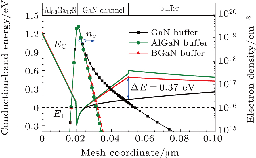
3. Results and discussionAt first, under zero applied voltage, the conduction-band profiles and electron distributions in the investigated structures are calculated by one-dimensional self-consistent simulation as shown in Fig. 3. In the AlGaN/GaN structure with a GaN buffer, the electrons are accumulated near the Al0.3Ga0.7N/GaN interface to form 2DEG by the columbic attraction of positive polarization charges. However, due to the poor confinement at the backside of the channel, the electrons of 2DEG can easily overflow into the GaN buffer and lead to a wide 2DEG distribution, which is not conducive to the gate-to-channel control. In particular, for the device with a short-gate in the pinch-off state, the depletion region under the gate is much smaller than that for the device with a long-gate,[30] resulting in the channel being difficult to pinch off and high buffer leakage current. If the B0.01Ga0.99N is used as a buffer, the sheet negative piezoelectric polarization charge at the GaN/BGaN interface can increase the barrier height of the backside of the channel by about 0.37 eV, thereby limiting the electrons of 2DEG to a smaller depth. In a sense, the negative polarization charge at the GaN/BGaN interface is more like a negative back-gate, which assists the top-gate to modulate the channel more efficiently. Since the sheet negative polarization charges at the GaN/B0.01Ga0.99N interface and the GaN/Al0.03Ga0.97N interface are similar in density, the ability of the B0.01Ga0.99N buffer to enhance 2DEG confinement is close to that of the Al0.03Ga0.97N buffer.
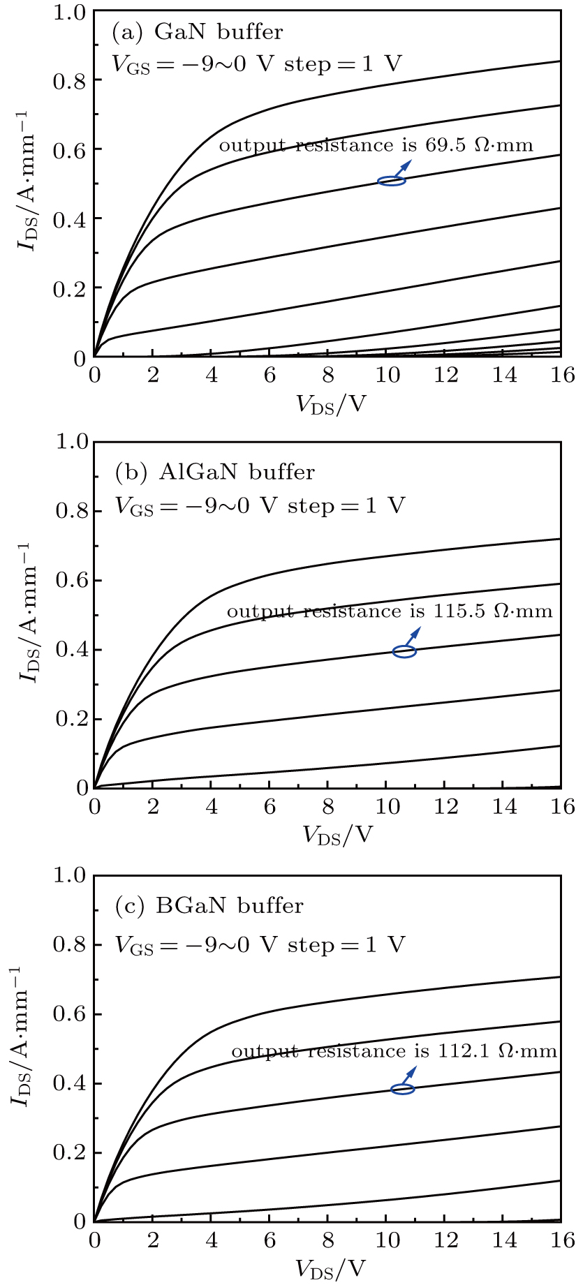
Figure 4 shows the calculated I–V output characteristics of the investigated devices. It can be clearly seen that the B0.01Ga0.99N buffer device has a significant improvement in the pinch-off quality compared with the GaN buffer one. A maximum drain current of
 is gained at VGS = 0 V in the BGaN buffer device, which is about 16% lower than that of the GaN buffer one (
 ). The reduction in drain current mainly results from the decrease in 2DEG density. Moreover, in the saturation region, the increase of output resistance in the BGaN buffer device means the suppression of SCEs. The maximum drain current and output resistance in the Al0.03Ga0.97N buffer device are
 and
and
 , respectively, which are similar to those in the B0.01Ga0.99N buffer device.
Figure 5(a) shows the transfer characteristics of the three devices at VDS = 5 V. In the B0.01Ga0.99N buffer device, the threshold voltage (−4.29 V) is shifted forward by about 1.0 V compared with that in the GaN buffer one (−5.33 V), which is mainly because the depletion of the negative polarization charge causes 2DEG density to decrease. In addition, since the tensile strain of the Al0.3Ga0.7N barrier layer grown on the completely lattice relaxed B0.01Ga0.99N or Al0.03Ga0.97N buffer is less than that of the GaN buffer structure, the density of positive piezoelectric charges at the Al0.3Ga0.7N/GaN interface slightly decreases, which is also a small part of reason for the 2DEG reduction. Since the lattice constant a of B0.01Ga0.99N is much smaller than the lattice constant a of Al0.03Ga0.97N (see Fig. 2), the 2DEG density of the B0.01Ga0.99N buffer structure is slightly lower than that of Al0.03Ga0.97N buffer device, which can explain that the B0.01Ga0.99N buffer device has a slightly larger threshold voltage than the Al0.03Ga0.97N buffer one. Comparing with the GaN device, the transconductance (Gm) in the BGaN buffer device decreases in the region from the initial conduction of the device to the peak, which mainly results from the subsequent higher threshold voltage and the higher access resistance caused by the decreasing of 2DEG density. This Gm characteristic can be seen commonly in the HEMTs with an AlGaN buffer.[19–21] However, due to the improved gate-to-channel control efficiency, the BGaN device has a steep change of Gm near the pinch-off region, which implies the low sub-threshold current and good pinch-off quality. To evaluate the SCEs in the devices, the drain-induced barrier lowering (DIBL) and sub-threshold swing (SS) value are calculated as shown in Fig. 5(b). The BGaN buffer device achieves a DIBL of 53 mV/V, and an SS (VDS = 4 V) of 134 mV/dec, which are much lower than the DIBL of 163 mV/V and SS (VDS = 4 V) of 534 mV/dec in the GaN buffer device. The ability of the B0.01Ga0.99N buffer device to control SCEs is not much different from that of the Al0.03Ga0.97N buffer device.
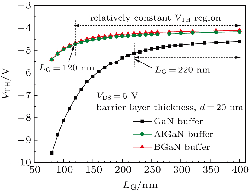
To further investigate the ability to control SCEs in the BGaN buffer HEMTs, the threshold voltage (VTH) is also simulated as a function of gate-length (LG) at VDS= 5 V as shown in Fig. 6. In the GaN buffer devices, when the gate-length is shortened to 220 nm (LG/d = 11), the shift in VTH will become apparent, which is consistent with the prediction that VTH remains relatively constant for the aspect ratio greater than 10.[4, 5] In comparison, the B0.01Ga0.99N buffer and the Al0.03Ga0.97N buffer devices can maintain relatively constant VTH at LG greater than 120 nm (LG/d = 6), which is much lower than the aspect ratio of the GaN buffer one.
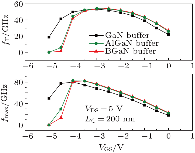
The RF performance of the three devices is also calculated by small-signal AC simulation. Figure 7 shows the current cutoff frequency (fT) and the power gain cutoff frequency (fmax) as a function of the gate voltage at VDS = 5 V. A peak fT of 53.8 GHz and fmax of 82.4 GHz are extracted in the BGaN buffer HEMT. There is only a small increase compared with the scenario of the GaN buffer HEMT (fT = 53.5 GHz, fmax =80 GHz). However, when the gate voltage exceeds the voltages at the peaks of fT and fmax, the RF performance of the BGaN buffer device is improved to varying degrees, which is mainly attributed to the decrease in the buffer leakage current that leads to larger output resistance. The RF performance of the Al0.03Ga0.97N and B0.01Ga0.99N buffer devices are substantially similar.
4. ConclusionsTo suppress SCEs, a B0.01Ga0.99N buffer is utilized to enhance 2DEG confinement in a short-gate AlGaN/GaN HEMT structure. Based on two-dimensional TCAD simulation, the DC and RF characteristics of the B0.01Ga0.99N buffer HEMT are theoretically studied. Comparing with the GaN buffer device, good pinched-off behavior and improved RF performance are obtained in the BGaN buffer device. As the gate length decreases, the BGaN buffer device with an LG/d of six has a good immunity to the shift of threshold voltage, which is much lower than that the GaN buffer device with LG/d = 11 possesses. Moreover, the B0.01Ga0.99N buffer device has similar dc and RF characteristics to those the AlGaN buffer device possesses, and its ability to control SCEs is comparable to that of Al0.03Ga0.97N buffer. Therefore, this BGaN buffer with very small B-content could be a new method to control SCEs. Therefore, this study provides a reference for the research of BGaN buffers.


