High quantum efficiency long-/long-wave dual-color type-II InAs/GaSb infrared detector
Jiang Zhi1, 2, Sun Yao-Yao1, 2, Guo Chun-Yan1, 2, Lv Yue-Xi1, 2, Hao Hong-Yue1, 2, Jiang Dong-Wei1, 2, Wang Guo-Wei1, 2, ‡, Xu Ying-Qiang1, 2, Niu Zhi-Chuan1, 2, †
State Key Laboratory for Superlattices and Microstructures, Institute of Semiconductors, Chinese Academy of Sciences, Beijing 100083, China
Center of Materials Science and Optoelectronics Engineering, University of Chinese Academy of Sciences, Beijing 100049, China


† Corresponding author. E-mail: zcniu@semi.ac.cn wangguowei@semi.ac.cn

Project supported by the National Key Technology R&D Program of China (Grant Nos. 2018YFA0209104 and 2016YFB0402403).

Abstract

A long-/long-wave dual-color detector with N-M-π-B-π-M-N structure was developed based on a type-II InAs/GaSb superlattice. The saturated responsivity was achieved under low bias voltage for both channels. The device could be operated as a single detector for sequential detection and showed high quantum efficiencies. The peak quantum efficiencies of long-wavelength infrared band-1 (blue channel) and long-wavelength infrared band-2 (red channel) were 44% at 6.3 μm under 20 mV and 57% at 9.1 μm under −60 mV, respectively. The optical performance for each channel was achieved using a 2 μm thickness absorber. Due to the high QE, the specific detectivities of the blue and red channels reached 5.0 × 1011 cm·Hz1/2/W at 6.8 μm and 3.1 × 1011 cm·Hz1/2/W at 9.1 μm, respectively, at 77 K.

1. Introduction

Type-II InAs/GaSb superlattices (T2SLs), first proposed by Sai-Halasz et al. in the 1970s,[1] offer an alternative means of infrared detection and imaging. Mercury-cadmium telluride (MCT) photodetectors have several issues: they are toxic, relatively costly, and can be inhomogeneous over large wafers. Long-wavelength infrared (LWIR) MCT photodetectors are often limited by Auger recombination, which T2SLs have been theorized to be able to suppress, which could potentially lead to better performance. Furthermore, T2SLs have already demonstrated high external quantum efficiencies (QEs) of up to 50% in the LWIR.[2] Infrared detectors with PπMN-structure[3,4] and unipolar barrier structure[5,6] have been developed. In those studies, T2SLs have shown flexibility in device structure design to improve the detector performance.[79] Multi-color/band detectors can contribute to enhancing image contrast or target recognition.[810] Detectors configured for LWIR/LWIR detection are used for clutter rejection in a wide variety of space and ground-based applications.[11,12]

In this work, a long-/long-wave dual-color detector with high QE based on an N-M-π-B-π-M-N structure was first developed. The blue and red channels with 50% cutoff wavelengths at 7.6 μm and 11.5 μm, respectively, presented QEs of 44% and 57% at 77 K. In the structure, the M-structure barrier was used to suppress the dark current. And in order to inhibit cross-talk, an Al0.2Ga0.8Sb layer was sandwiched between the blue and the red channels.

2. Experiment
2.1. Material and structure

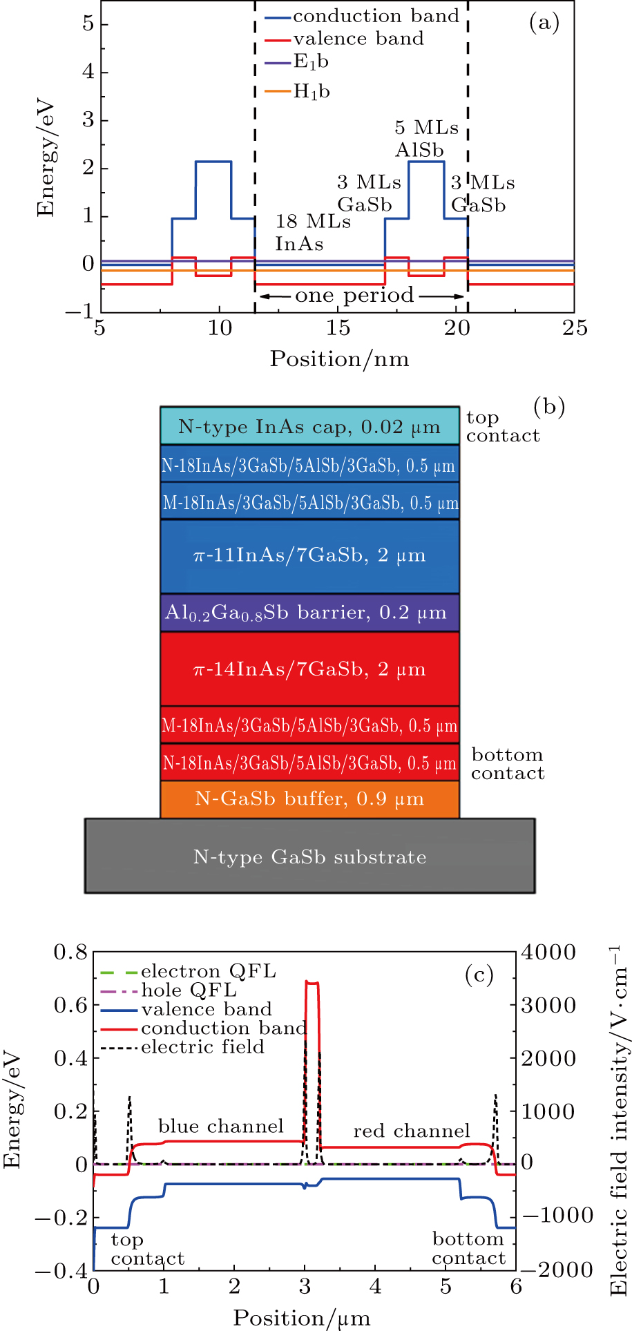
The band structure of the M-structure superlattice is shown in Fig. 1(a). Its periodic structure was composed of 18 monolayers (MLs) InAs/3 MLs GaSb/5 MLs AlSb/3 MLs GaSb. The thin AlSb layer in the M-structure affects both electrons in the conduction band and holes in the valence band. It forms a more effective barrier that blocks the tunneling of the electrons in the two adjacent InAs wells. For holes, the AlSb layer causes the GaSb layer to become a double quantum well, which elevates the first and the second valence bands. Therefore, with the high electron effective mass in the M-structure, the transport of electrons in the depletion region due to diffusion and tunneling would have more resistance, and the dark current is expected to decrease.[3] Our device was grown using a molecular beam epitaxy (MBE) system (Veeco Epi Gen II) based on an N-type GaSb (100) substrate. The substrate was double-side polished to avoid strain relaxation and interface related defects.[13] The structure and band diagram of the device are shown in Fig. 1(b). First, an N-type GaSb buffer with thickness of 900 nm was grown between the substrate and the red channel contact region, which ensures an atomically smooth surface for the device growth. Then, the 2 μm thick lightly Be-doped (p ≈ 4–6 × 1016 cm−3) active region superlattice for the red channel was grown with 14 MLs of InAs and 7 MLs of GaSb per period, while the blue channel grown subsequently had an 11 MLs InAs/7 MLs GaSb design with the same total thickness. Both Si-doped N regions (n ≈ 1 × 1018 cm−3) were composed of a 0.5 μm thick M-superlattice. The M-structure barrier regions with thickness of 0.5 μm were undoped. A 0.2 μm Be-doped (p ≈ 8 × 1016 cm−3) Al0.2Ga0.8Sb barrier was sandwiched between the two channels. Finally, the entire structure was capped off with a 0.02 μm thick N-type (n ≈ 2 × 1018 cm−3) InAs layer.

Fig. 1. (a) The band diagram of the M-structure, where E1b and H1b represent the band edges of the first electron energy levels and the first hole energy levels in the minibands, respectively. (b) The structure diagram and (c) band alignment of the LW/LW dual-color detector, where the electron QFL and hole QFL represent quasi Fermi levels.

The band alignment and distribution of electrical field intensity are shown in Fig. 1(b). The valence band offset between the red and blue channels was almost eliminated. This means that the device could be operated under low bias voltage. The electrical field drop is small across both absorber regions, since there is a significant amount of field drop across the wider-bandgap barrier layers. This reduction in electric field will lead to small depletion regions and hence a reduction in the generation–recombination current (Jgr) and tunneling current.

The mismatch of each superlattice was measured using symmetric (004) x-ray diffraction. The high-resolution x-ray diffraction (HRXRD) pattern is shown in Fig. 2(a). Table 1 lists the parameters of each superlattice in the device. All of the contained superlattices’ periodic thicknesses match well with our design. The full width at half maximum (FWHM) shows the high crystalline quality of the epi-layers. The morphology of the sample was characterized by differential interference microscopy (Nikon ECLIPSE) (Fig. 2(b)) and atomic force microscopy (AFM) (Fig. 2(c)). In an area of 870 μm × 650 μm, the epi-layer exhibits flatness and non-defective morphology. The AFM scanning result shows the atomic step edge. And the root-mean-square (RMS) of roughness is 1.9 Å over a 10 μm × 10 μm area.

Fig. 2. (a) HRXRD pattern, (b) differential interference micrograph, and (c) AFM image of the device.
Table 1.

The mismatch, period, and FWHM of 0th peaks of different superlattices.

.
2.2. Device fabrication

The mesas with different sizes (200 μm, 300 μm, 500 μm) were defined through lithography (SUSS MA6) and fabricated by dry etching through the InAs cap layer (top contact) and each region into the red channel N-type contact (bottom contact). The SiO2 hard etching mask (PECVD STS) and inductively coupled plasma (ICP OXFORD plasmalab System 100) system were chosen to etch the mesa. The sidewall was passivated using anodic sulfide, then covered by a 200 nm SiO2 layer. The SiO2 layer was deposited using ion beam sputtering (OXFORD optofab3000). After the above steps, a second photolithography and ICP were performed to open the window on the passivation layer. The final metal electrode was deposited using electron beam evaporation (SKY EB700-I).

3. Results and discussion
3.1. Spectral response

The working mechanism is similar to that of the dual-band detector which was mentioned in Ref. [14]. The optical characterization of the front-side illuminated detector was performed at 77 K using a Fourier transform infrared (FTIR) spectrometer (Bruker Vertex70) and a calibrated black-body (SYSTEMS) source at a temperature of 500 °C. The FTIR spectrometer was calibrated by using a standard DTGS detector without anti-reflection (AR) coating. Figure 3 shows the optical performance of the detector with diameter 300 μm. It is defined as forward bias when the applied bias on the top contact is positive with respect to the bottom contact. Otherwise, it is defined as reverse bias. The blue channel exhibits a peak responsivity (Ri) of 2.4 A/W at 6.8 μm under 20 mV, while the red channel shows a peak Ri of 4.2 A/W at 9.1 μm under a bias of −60 mV. The 50% QE cutoff wavelengths are measured at 7.6 μm and 11.5 μm. The peak QEs of the blue and red channels are 44% at 6.3 μm and 57% at 9.1 μm, respectively. From Fig. 3(c), the bias range above −20 mV corresponds to the transport of minority electrons in the blue channel, while the bias range below −20 mV corresponds to the transport of minority electrons in the red channel. The applied bias is small enough to be suitable for focal plane arrays (FPAs) operation. In order to quantify the optical cross-talk, we use a selectivity parameter (S) defined as follows:[15]

where , , , and are the QEs of the blue and red channels at 9.1 μm and 6.3 μm, respectively. Using these parameters, the selectivities of the blue and red channels are 0.46 and 0.02, respectively. The low Sblue demonstrates that the photoexcited electrons in the red channel are blocked by the Al0.2Ga0.8Sb barrier. The Sred is poor because the 2 μm thick absorber of the blue channel means it is hard to fully suppress the response of the red channel below 8 μm. Under a bias of −50 mV, the detector shows the lowest Sred of 0.21. Assuming there is no internal reflection inside the device, we can estimate how much IR signal is stopped by the blue channel. The blue channel blocks 60% of the IR radiation between 3 μm and 8 μm. The optical cross-talk can be effectively suppressed by increasing the absorber thickness. Table 2 lists the published results and our result; the performance of our single-unit device approaches, or even surpasses, that of the previous ones.

Fig. 3. (a) Spectral responsivity and (b) quantum efficiency under −60 mV, −20 mV, and 20 mV at 77 K. (c) The variation of quantum efficiency with applied bias for wavelengths of 9.1 μm and 6.3 μm at 77 K.
Table 2.

Comparison with published results.

.
3.2. The IV characterization

The dark current density (J) was measured using Agilent B1500 in the bias range from 0.3 V to −0.3 V at 77 K. As shown in Fig. 4(a), the blue and red channels of the device with diameter 300 μm show dark currents of 8.5 × 10⁻⁵ A/cm2 at 20 mV and 4.6 × 10⁻⁴ A/cm2 at −60 mV, respectively. The differential resistance and area products RA are 201 Ω ·cm2 under 20 mV and 67 Ω ·cm2 under −60 mV at 77 K. The linear fitting of inverse RA vs. P/A is shown as a function of P/A for the devices with diameter 500 μm, 300 μm, and 200 μm in Fig. 4(b), and the bulk-limited resistances of the blue and red channels are 1000 Ω · cm2 and 179 Ω ·cm2, respectively. The surface resistivity is equal to 2.9 × 10⁴ Ω · cm and 9.1 × 10³ Ω · cm for the blue and red channels, respectively, at 77 K. For both channels, the relatively high surface resistivity shows suppressed surface related currents, but the bulk-limited resistance is not large enough to block the bulk leakage.[12] As a result, the main dark current comes from bulk leakage. Compared with the results published in Refs. [11] and [12], the dark current density of our blue channel is relatively high. The bulk leakage was fitted by referencing the published result.[16] As shown in Fig. 4(c), the main leakage in both channels under operating bias is Jgr. The M-structure barrier in the blue channel fails to take most part of the applied bias. Therefore, a large part of the p-side depletion region lies within the absorber layer, giving rise to large Jgr. A narrow width of the depletion region in the absorber is beneficial for decreasing Jgr. It may be useful to decrease the depletion region width in the blue channel by using the periodic structure of 18 MLs InAs/5 MLs GaSb/5 MLs AlSb/5 MLs GaSb to replace the currently used M-structure. And the high density of recombination centers in the absorber also results in large Jgr. Another main dark current source is the trap-assisted tunneling current (JTAT) that depends on the trap density and the effective mass of the electrons. And in theory, the recombination centers and trap states can be eliminated by optimizing the superlattices’ growth conditions.

Fig. 4. (a) Dark current density J, differential resistance and area products RA of the dual-color detector with mesa diameter 300 μm. (b) The inverse RA vs. P/A is shown as a function of P/A for the detectors with different sizes. (c) Measured and modeled dark current of the LW/LW dual-color detector under bias from −0.3 V to 0.3 V.

Figure 5(a) collects dark current densities of the blue and red channels for comparison with “Rule 07”. The cutoff wavelength is taken as the point of a 50% response. The experimental data of the blue channel show considerably greater leakage current than Rule 07 by some orders of magnitude, while the current density of the red channel is close to Rule 07. The trend is that it is generally more difficult to control dark current at the shorter wavelength.[17] The specific detectivity (D*) spectrum is shown in Fig. 5(b). At 77 K, the maximum D* for the blue channel is 5.0 × 1011 cm·Hz1/2/W at 6.8 μm under 0 mV, while the red channel has 3.1 × 1011 cm·Hz1/2/W at 9.1 μm under −60 mV. The specific detectivity can be enhanced by increasing the absorber thickness and inhibiting dark current density.

Fig. 5. (a) The 77 K dark current densities plotted against cutoff wavelength for the blue channel under 20 mV and the red channel under −60 mV. The solid line indicates the dark current density calculated using the empirical Rule 07 model. (b) The specific detectivity spectrum of both channels at different applied bias voltages.
4. Conclusion and perspectives

In this work, a long-/long-wave dual-color detector based on an InAs/GaSb superlattice with N-M-π-B-π-M-N structure was successfully fabricated and characterized. The peak QEs of the blue and red channels are 44% at 6.3 μm under 20 mV and 57% at 9.1 μm under −60 mV, respectively. And the corresponding responsivities of the blue and red channels are 2.4 A/W at 6.8 μm and 4.2 A/W at 9.1 μm, respectively. The optical performance was measured based on a 2 μm thick absorber. The maximum D* for the blue channel is 5.0 × 1011 cm·Hz1/2/W at 6.8 μm without applied bias, while it is 3.1 × 1011 cm·Hz1/2/W at 9.1 μm under −60 mV for the red channel. In order to achieve better performance, the device structure and fabrication process of the dual-color detector both need to be further optimized.

Reference
[1] Sai-Halasz G A Tsu R Esaki L 1977 Appl. Phys. Lett. 30 651
[2] Nguyen B M Hoffman D Wei Y J Delaunay P Y Hood A Razeghi M 2007 Appl. Phys. Lett. 90 231108
[3] Nguyen B M Hoffman D Delaunay P Y Razeghi M 2007 Appl. Phys. Lett. 91 163511
[4] Huang E K Pour S A Hoang M A Haddadi A Razeghi M Tidrow M Z 2012 Opt. Lett. 37 2025
[5] Ting D Z Hill C J Soibel A Keo S A Mumolo J M Nguyen J Gunapala S D 2009 Appl. Phys. Lett. 95 023508
[6] Rodriguez J B Plis E Bishop G Sharma Y D Kim H Dawson L R Krishna S 2007 Appl. Phys. Lett. 91 043514
[7] Han X Xiang W Hao H Y Jiang D W Yao Y Wang G W Xu Y Q Niu Z C 2017 Chin. Phys. 26 018505
[8] Jiang Z Han X Sun Y Y Guo C Y Lv Y X Hao H Y Jiang D W Wang G W Xu Y Q Niu Z C 2017 Infrared Phys. Technol. 86 159
[9] Jiang D W Xiang W Guo F Y Hao H Y Han X Li X C Wang G W Xu Y Q Yu Q J Niu Z C 2016 Chin. Phys. Lett. 33 048502
[10] Sun Y Y Lv Y X Han X Guo C Y Jiang Z Hao H Y Jiang D W Wang G W Xu Y Q Niu Z C 2017 Chin. Phys. 26 098506
[11] Huang E K Razeghi M 2012 SPIE Proceedings - The International Society for Optical Engineering 21–26 January 2012 San Francisco, United States 82680Z 10.1117/12.913662
[12] Plis E Myers S A Ramirez D A Krishna S 2016 SPIE Defense + Security 17–21 April 2016 Baltimore, United States 981911 10.1117/12.2228166
[13] Rodriguez J B Christol P Cerutti L Chevrier F Joullié A 2005 J. Cryst. Growth 274 6
[14] Ariyawansa G Grupen M Duran J M Scheihing J E Nelson T R Eismann M T 2012 J. Appl. Phys. 111 073107
[15] Razeghi M Haddadi A Dehzangi A Chevallier R Yang T 2017 SPIE Defense + Security 9–13 April 2017 Anaheim, United States 1017705 10.1117/12.2267044
[16] Martyniuk P Wrobel J Plis E Madejczyk P Kowalewski A Gawron W Krishna S Rogalski A 2012 Semicond. Sci. Technol. 27 055002
[17] Rogalski A Martyniuk P Kopytko M 2017 Appl. Phys. Rev. 4 031304