Graphene-like Be3X2 (X = C, Si, Ge, Sn): A new family of two-dimensional topological insulators
Song Lingling1, Zhang Lizhi2, Guan Yurou1, Lu Jianchen1, Yan Cuixia1, †, Cai Jinming1, ‡
Faculty of Materials Science and Engineering, Kunming University of Science and Technology, Kunming 650093, China
Institute of Physics, Chinese Academy of Sciences, Beijing 100190, China


† Corresponding author. E-mail: j.cai@kmsut.edu.cn cuixiayan09@gmail.com

Abstract

Using first-principle calculations, we predict a new family of stable two-dimensional (2D) topological insulators (TI), monolayer Be3X2 (X = C, Si, Ge, Sn) with honeycomb Kagome lattice. Based on the configuration of Be3C2, which has been reported to be a 2D Dirac material, we construct the other three 2D materials and confirm their stability according to their chemical bonding properties and phonon-dispersion relationships. Because of their tiny spin–orbit coupling (SOC) gaps, Be3C2 and Be3Si2 are 2D Dirac materials with high Fermi velocity at the same order of magnitude as that of graphene. For Be3Ge2 and Be3Sn2, the SOC gaps are 1.5 meV and 11.7 meV, and their topological nontrivial properties are also confirmed by their semi-infinite Dirac edge states. Our findings not only extend the family of 2D Dirac materials, but also open an avenue to track new 2DTI.

1. Introduction

Two-dimensional (2D) Dirac materials, with a linear band dispersion around the Fermi level and massless carriers that can be described by Dirac equations,[1,2] displaying ballistic charge transport and enormously high carrier mobility, exhibiting special topological phases,[311] will offer potential applications for high performance electronic and spintronic devices. However, the Dirac cores in most of these 2D materials can only exist in the absence of spin–orbit coupling (SOC).[12] The SOC will open a gap at the Dirac point and lead to a topological insulating phase, especially when the SOC strength is very strong.[7,13] The 2D topological insulators (TI) exhibit the quantum spin Hall effect with spin-filtered edge states in their bulk SOC gaps.[14,15] In general, if the SOC gap is very small (< 1 meV, e.g., the SOC gap for graphene is about 0.0008 meV),[16] the influence of the SOC will be neglected, and it will be considered that the 2D material is a “real” 2D Dirac material with linear band dispersion around the Fermi level.[17] If the SOC gap is large (> 1 meV), the 2D Dirac materials will be 2DTI.[18,19] Then, the 2D Dirac materials are more likely composed of light elements (e.g., B, C, N) and the 2DTI are more likely constructed by heavy elements (e.g., Sn, Pb, Bi). Up to now, lots of 2D Dirac materials (or 2DTI) have been predicated and investigated, which include graphene,[1] silicene,[18,20] germanene,[18,20] several kinds of graphynes,[2123] topological insulators on semiconductor surfaces,[46,911] 2D organic TI,[68] and so on. Especially for graphene, as the only 2D Dirac material that has been truly confirmed in experiment, it has attracted intense interest over the past decade.[1,24]

Graphene, graphynes, and silicene are all single-element materials. Compare to these single-element materials, bi-element materials have more complex structures and more potential to be modulated. Up to now, lots of bi-element 2D Dirac materials and 2DTI have been predicted and investigated, e.g., polyaniline (C3N),[25] C4N-I,[25] C4N-II,[25] TiB2,[26] and MC6 (M = Mo, W).[27] Recently, Wang et al. have predicted a new 2D Dirac material, monolayer Be3C2, by using the global particle-swarm optimization method and density functional theory.[28] We know that the group IV elemental monolayers have played a crucial role in the field of 2D materials, where graphene (C) is a Dirac material, silicene (monolayer Si),[18,20] germanene (monolayer Ge),[18,20] and stanene (monolayer Sn) are topological insulators.[29] Then, what is the stability and electronic properties of the Be3X2 (X = Si, Ge, Sn)?

In this work, by using first-principle calculations, we investigated the stability and electronic properties of honeycomb Kagome (HK) mixed 2D materials Be3X2 (X = C, Si, Ge, Sn), and found that all of them are 2DTI. More interestingly, monolayer Be3C2 and Be3Si2 have very tiny SOC gaps (< 1 meV), which means that both are 2D Dirac materials. According to the semi-infinite Dirac edge states of these four materials, we can confirm that Be3Ge2 and Be3Sn2 are 2DTI, and their SOC gaps are much larger than those of Be3C2 and Be3Si2.

2. Computational details

The density-functional calculations are performed by using the plane wave basis Vienna ab initio simulation pack (VASP).[30] The projector-augmented plane wave (PAW) approach is used to represent the ion–electron interaction.[31] The Perdew–Burke–Ernzerhof (PBE) generalized gradient approximation is adopted for the electron–electron interactions.[32] The energy cutoff of the plane wave is set to 600 eV with a precision energy of 10−4 eV/atom and a precision force of.01 eV/Å. The Monkhorst–Pack scheme with 15×15×1 and 95×95×1 k-points is used to sample the Brillouin zone for structural optimization and self-constant electronic properties calculation, respectively. In all the calculations, the 18 Å vacuum layer is used to avoid the spurious interactions between periodic images. To assess the dynamical stability, phonon dispersions are calculated based on the finite displacement method which is embedded in the phonopy program.[33,34] The semi-infinite Dirac edge states are calculated by using the Wannier90 package.[35,36]

3. Results and discussion
3.1. Geometrical properties and structural stabilities

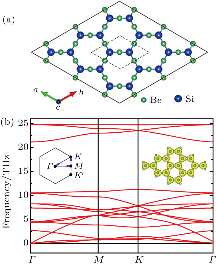
A geometrical configuration of monolayer Be3Si2 is shown in Fig. 1(a), which has the same lattice as that of Be3C2, the HK lattice, where it is composed of a hexagonal lattice formed by the Si atoms and a Kagome lattice formed by the Be atoms. From this figure, we can find that there are three Be and two Si atoms in its unit cell, with a Be–Si bond length of 2.12 Å. Due to sp2 orbital hybridizations, each Si atom bonds with three Be atoms by using a strong σ-bond, and the final pz electrons make up the π-bond. In addition, we also calculate the phonon dispersion curves of the monolayer Be3Si2, as shown in Fig. 1(b). An absence of imaginary frequencies demonstrates dynamical stabilities of the Be3Si2 structure. For Be3Ge2 and Be3Sn2, both have the same geometrical structure as that of Be3Si2, but their lattice constants are different (shown in Table 1), where the bond length of Be–Ge is 2.14 Å, and the bond length of Be–Sn is 2.34 Å. Meanwhile, an absence of imaginary frequencies in the phonon dispersion curves of Be3Ge2 and Be3Sn2 (Fig. S1) also demonstrates their dynamical stability. We also performed ab initio molecular dynamics (MD) simulations using a supercell of 3×3 unit cells at 300 K up to 5 ps and confirmed that these three structures are stable (see Figs. S1(c)–S1(e) in the supporting information). To reveal the bonding nature of monolayer Be3Si2, we calculate the electron localization function (ELF),[37,38] which is shown in the right inset of Fig. 1(b). The high ELF value between Be atoms and Si atoms indicates a strong covalent bond between them, which stabilizes the 2D monolayer Be3Si2.

Fig. 1. (a) Optimized configuration of Be3Si2 monolayer with a unit cell labeled by black dashed line. The green and blue spheres represent Be and Si, respectively. (b) Phonon-dispersion curves, where the left inset indicates the first Brillouin zone, and the right inset shows the electron localization function of the Be3Si2 monolayer with the iso-value of 0.96.
Table 1.

Lattice constants a, band gaps within SOC Eg, and Fermi velocities VF of graphene, silicene, and Be3X2

.
3.2. Electronic properties and Dirac states of Be3Si2

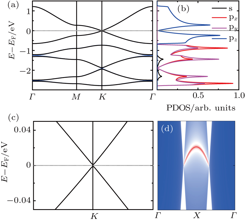
To investigate the electronic properties of monolayer Be3Si2, we calculate its band structures and corresponding projected density of states (PDOS), as shown in Fig. 2. From its band structure, we can find that there are two linear bands crossing at the Fermi level, which is a typical type of Dirac material, where the Dirac point just locates at the high-symmetry K point. The PDOS shows that the Dirac states near the Fermi level are mainly contributed to by the pz orbital of Si, which can be indicated by real space charge distributions of the highest occupied band (HOB) and the lowest unoccupied band (LUB) of Be3Si2 (Figs. 2(c) and 2(d)). We also provide the three-dimensional valence and conduction bands in Fig. 2(b), which clearly shows the features of the Dirac cone in its first Brillouin zone. The linear dispersion of the energy bands suggests that the effective mass of the carriers near the Fermi level is zero (the effective mass of charge carriers is defined as m* = (d2E/dk2)−1). The calculated Fermi velocity is about 5.7×10⁵ m/s, and the linear dispersion maintains until about ±0.25 eV away from the Dirac point. Both are close to one-half of that in freestanding graphene.[39] Therefore, the Be3Si2 monolayer is expected to have ultra-high carrier mobility and excellent electronic transport properties.

Fig. 2. Electronic structures of Be3Si2: (a) band structure and PDOS, (b) 3D valence and conduction bands around the Fermi level, (c) and (d) the real space charge distributions of HOB and LUB.

Mostly, Dirac cores can only exist in the absence of SOC.[12] But Be3C2 can be considered as 2D Dirac materials even with SOC, because its SOC gap is very small (0.04 meV).[28] For Be3Si2, the SOC can open a tiny band gap of 0.06 meV, being also much smaller than 1 meV, which means that Be3Si2 is one new “real” 2D Dirac material. We know that silicene is a 2DTI with a SOC band gap about 1.55 meV.[18] The large SOC gap comes from buckled properties of silicene, where some of the in-plane orbitals contribute to the bands around the Fermi level.[20] Here, there is no buckle for Be3Si2, and only the pz orbitals (out of plane orbitals) of Si contribute to the bands around the Fermi level. Similar to graphene and Be3C2, Be3Si2 has a very small SOC gap, which leads it to be a 2D Dirac material.

3.3. Topological properties of Be3X2

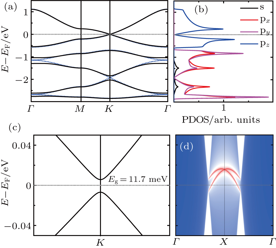
In Fig. 3(a), we provide a zoom-in band structure with SOC of Be3Si2 around the Fermi level, where we can clearly find the linear dispersion relationship. To calculate the topological edge states, we firstly fit a tight binding Hamilton based on the largest localized Wannier function (MLWF) according to the DFT band structure.[36] Then, by using the MLWFs, we build the edge Green’s function of the semi-unique lattice by using recursive methods and calculate the local density of states (LDOS) (shown in Figs. 3(b), 4(d), and 5(d)).[36] According to our calculation results, we can find that nontrivial topological edge states connect the bulk bands. For Be3Si2, due to the tiny SOC gap, the two time-reversal-symmetry bands (Dirac bands of the edge states) around the Fermi level nearly degenerate, and it seems that there is an arc connecting the two Dirac points (Fig. 3(b)). For Be3Ge2 and Be3Sn2, without SOC, they have similar band structures to that of Be3Si2 (Figs. 4(a) and 5(a)). However, with SOC, because the SOC strengths of Ge and Sn are much larger than that of C, their SOC band gaps are 1.5 meV and 11.7 meV, respectively, and both are 2DTI. We also use the HSE06 method to calculate the SOC band gaps of these three structures and find that their band gaps are 0.34 meV, 1.55 meV, and 18.9 meV, respectively. In Figs. 4(c) and 5(c), we provide their zoom-in band structures with SOC around the Fermi level, where we can clearly see the SOC gaps at the Dirac points. In Figs. 4(d) and 5(d), we can clearly find the semi-infinite edge states within the SOC gaps, then we can confirm that that they are both intrinsic 2DTI with larger SOC gaps than Be3C2 and Be3Si2 (Figs. 4(d) and 5(d)).

Fig. 3. (a) Band structures of Be3Si2 with SOC around K points, where the inset is the zoom-in view around the Fermi level. (b) The semi-infinite Dirac edge states around the Fermi level.
Fig. 4. Electronic properties of Be3Ge2. (a) Band structures with (black line) and without (blue dash) SOC. (b) Projected density of states without considering SOC. (c) Zoom-in figure around K points of the band structures considering the SOC. (d) The semi-infinite Dirac edge states around the Fermi level.
Fig. 5. Electronic properties of Be3Sn2. (a) Band structures with (black line) and without (blue dash) SOC. (b) Projected density of states without considering SOC. (c) Zoom-in figure around K points of the band structures considering the SOC. (d) The semi-infinite Dirac edge states around the Fermi level.

More interestingly, for Be3Sn2, its deep energy bands exhibit much larger SOC band gaps (∼0.2 eV) and semi-infinite Dirac edge states (Fig. S2). These large SOC band gaps mean that we can realize a large gap 2DTI if we move the Fermi level to these gaps by hole doping.

4. Conclusion

We investigate a family of 2DTI with HK lattice, monolayer Be3X2 (X = C, Si, Ge, Sn). Based on the chemical bonding properties and phonon-dispersion relationships, we have confirmed their stabilities. By investigating their electronic and topological properties, we find that Be3C2 and Be3Si2 can be considered as 2D Dirac materials because of their tiny SOC band gaps. For Be3Ge2 and Be3Sn2, the SOC gaps are 1.5 meV and 11.7 meV, and their topological nontrivial properties are also confirmed by their semi-infinite Dirac edge states. Since the atomic numbers of the Ge and Sn atoms are larger than those of the C and Si atoms, the spin–orbit coupling effect is larger. Our research will enrich the family of 2DTI and promote the development of 2D materials.

Reference
[1] Castro Neto A H Guinea F Peres N M R Novoselov K S Geim A K 2009 Rev. Mod. Phys. 81 109
[2] Novoselov K 2007 Nat. Mater. 6 720
[3] Wang Z F Liu Z Liu F 2013 Nat. Commun. 4 1471
[4] Zhou M Ming W Liu Z Wang Z Li P Liu F 2014 Proc. Natl. Acad. Sci. USA 111 14378
[5] Zhu F F Chen W J Xu Y Gao C L Guan D D Liu C H Qian D Zhang S C Jia J F 2015 Nat. Mater. 14 1020
[6] Zhang L Z Zhai F Jin K H Cui B Huang B Wang Z Lu J Q Liu F 2017 Nano Lett. 17 4359
[7] Kane C L Mele E J 2005 Phys. Rev. Lett. 95 226801
[8] Zhang L Z Wang Z F Huang B Cui B Wang Z Du S X Gao H J Liu F 2016 Nano Lett. 16 2072
[9] Huang B Jin K H Zhuang H L Zhang L Liu F 2016 Phys. Rev. 93 115117
[10] Li P Zhou M Zhang L Guo Y Liu F 2016 Nanotechnology 27 095703
[11] Chuang F C Hsu C H Huang Z Q Kuo C C Liu Y T Lin H Bansil A 2015 New J. Phys. 17 025005
[12] Young S M Kane C L 2015 Phys. Rev. Lett. 115 126803
[13] Kane C L Mele E J 2005 Phys. Rev. Lett. 95 146802
[14] Qi X L Zhang S C 2011 Rev. Mod. Phys. 83 1057
[15] Schumayer D Hutchinson D A W 2011 Rev. Mod. Phys. 83 769
[16] Yao Y Ye F Qi X L Zhang S C Fang Z 2007 Phys. Rev. 75 041401
[17] Mayorov A S Elias D C Mukhin I S Morozov S V Ponomarenko L A Novoselov K S Geim A K Gorbachev R V 2012 Nano Lett. 12 4629
[18] Liu C C Feng W Yao Y 2011 Phys. Rev. Lett. 107 076802
[19] Dai X 2016 Physics 12 5
[20] Cahangirov S Topsakal M Akturk E Sahin H Ciraci S 2009 Phys. Rev. Lett. 107 076802
[21] Malko D Neiss C Vines F Goerling A 2012 Phys. Rev. Lett. 108 086804
[22] Xu L C Wang R Z Miao M S Wei X L Chen Y P Yan H Lau W M Liu L M Ma Y M 2014 Nanoscale 6 1113
[23] Zhang L Z Wang Z F Wang Z M Du S X Gao H J Liu F 2015 J. Phys. Chem. Lett. 6 2959
[24] Cheng H E Ming-Hui L U Chen Y F 2008 Physics 1 16
[25] Li L Kong X Leenaerts O Chen X Sanyal B Peeters F M 2017 Carbon 118 258
[26] Zhang L Z Wang Z F Du S X Gao H J Liu F 2014 Phys. Rev. 90 161402
[27] Liu P F Wu Y Bo T Hou L Xu J Zhang H J Wang B T 2018 Phys. Chem. Chem. Phys. Pccp 20 732
[28] Wang B Yuan S Li Y Shi L Wang J 2017 Nanoscale 9 5577
[29] Xu Y Yan B Zhang H J Wang J Xu G Tang P Duan W Zhang S C 2013 Phys. Rev. Lett. 111 136804
[30] Stadler R Wolf W Podloucky R Kresse G Furthmã¼Ller J Hafner J 1996 Phys. Rev. 54 1729
[31] Kresse G Joubert D 1999 Phys. Rev. 59 1758
[32] Perdew J P Burke K Ernzerhof M 1996 Phys. Rev. Lett. 77 3865
[33] Parlinski K Li Z Q Kawazoe Y 1997 Phys. Rev. Lett. 78 4063
[34] Togo A Oba F Tanaka I 2008 Phys. Rev. 78 134106
[35] Mostofi A A Yates J R Pizzi G Lee Y S Souza I Vanderbilt D Marzari N 2014 Comput. Phys. Commun. 185 2309
[36] Wu Q S Zhang S N Song H F Troyer M Soluyanov A A 2018 Comput. Phys. Commun. 224 405
[37] Becke A D Edgecombe K E 1990 J. Chem. Phys. 92 5397
[38] Savin A Jepsen O Flad J Andersen O K Preuss H Von Schnering H G 1992 Angew. Chem. 31 187
[39] Wallace P R 1947 Phys. Rev. 71 622