† Corresponding author. E-mail:
Project supported by the National Key Research and Development Program of China (Grant No. 2016YFB0400904), the National Natural Science Foundation for Distinguished Young Scholars, China (Grant No. 61725403), the National Natural Science Foundation of China (Grant Nos. 61574142, 61322406, 61704171, and 11705206), the Key Program of International Partnership Program of the Chinese Academy of Sciences (Grant No. 181722KYSB20160015), the Special Project for Inter-government Collaboration of State Key Research and Development Program, China (Grant No. 2016YFE0118400), the Science and Technology Service Network Initiative of the Chinese Academy of Sciences, the Jilin Provincial Science & Technology Department, China (Grant No. 20180201026GX), the Interdisciplinary Innovation Team of the Chinese Academy of Sciences, and the Youth Innovation Promotion Association of the Chinese Academy of Sciences (Grant No. 2015171).
Ultraviolet (UV) photodetectors based on wide band gap semiconductor have attracted much attention for their small volume, low working voltage, long lifetime, good chemical and thermal stability. Up to now, many researches have been done on the semiconductors based UV detectors and some kinds of detectors have been made, such as metal–semiconductor–metal (MSM), Schottky, and PIN-type detectors. However, the sensitivity values of those detectors are still far from the expectation. Recent years, surface plasmon (SP) has been considered to be an effective way to enhance the sensitivity of semiconductor based UV photodetector. When the light is matched with the resonance frequency of surface plasmon, the localized field enhancement or scattering effect will happen and thus the spectral response will be enhanced. Here, we present an overview of surface plasmon enhancing the performance of UV detectors, including the GaN, ZnO, and other wide band gap semiconductor UV detectors. Both fundamental and experimental achievements are contained in this review.
The UV detector has attracted much attention because of its wide potential applications in both civil and military, such as medical analysis, flame sensors, missile warning, ozone monitoring, and even UV astronomy in recent years.[1–4] The UV detectors based on third-generation semiconductors, such as GaN and their alloys Al(In)GaN, own the properties of direct band gap, thermal and chemical stability, making them have the merits of small volume, low working voltage, low energy consumption, long lifetime, high temperature resistant, and good anti-irradiation stability, so they have attracted more and more attention.
Up to now, great progress has been made of wide band semiconductor UV detectors, and some kinds of UV detectors have been fabricated, such as Schottky-type,[5] metal–semiconductor–metal (MSM)-type,[6] and p–n/p–i–n-type[7] detector. However, all of these detectors have no gain and thus cannot detect any weak signal. Avalanche photodiodes (APD) UV detectors can achieve high sensitivity, and they even can detect a single photo, but very strict quality material and fabrication process are required. The researchers have tried many approaches to improve the device performance,[8] and made a lot of progress but their responsivity values are still far from the expectation. In recent years, surface plasmon has provided new approaches to realizing high-sensitivity UV detectors.
The phenomenon of plasmon has a long history. The Lycurgus cup fabricated in fourth-century is the most ancient and famous exhibition, whose glass looks green in reflected light but ruby red in transmitted light. It has been shown that the dichroic glass contains a very small quantity of gold–silver alloy nanocrystals at a fraction of less than 1%.[9] The popular stained glass in the Middle Ages is also largely due to the nanoplasmonic resonance. In 1902, Robert Wood observed anomalous diffraction in a metal grating for the first time. However, he could not explain this phenomenon at that time.[10] Mie proposed a scattering theory of spherical nanoparticles (NPs) in 1908, the famous Mie’s theory which has become the theoretical basis for studying the surface plasmon properties of spherical metal nanoparticles.[11] Until 1941, Fano used the metal/air interface electromagnetic wave model to explain the anomalous diffraction observed by Wood.[12] Pines proposed in 1956 that the collective resonance of free electrons in metal should causes the energy to rapidly lose when the electrons propagated in the metal, and referred to the resonant electrons as “Plasmons”.[13] In 1957, Ritchie studied the energy loss of high-energy electrons during the propagation in metal thin film. He first proposed the concept of “Surface plasmonics” that describes the longitudinal fluctuation of electron density in metal.[14]
With the improvement of theory and processing technology, surface plasmon can have many applications such as in optoelectronic devices,[15,16] photocatalytic enhancement,[17,18] biological sensor,[19–21] and super resolution imaging.[22–24] Recent years, SP enhanced semiconductor optoelectronic devices like LEDs, solar cells and photodetectors,[25–27] have received more and more attention. In 2004, Okamoto systematically studied the coupling of enhanced luminescence by using three different metal films (silver, aluminum, and gold) evaporated on a quantum well.[28] The results showed that aluminum (Al) and silver (Ag) increased the photoluminescence (PL) peak intensity of InGaN/GaN quantum wells 8 and 14 times respectively. Lai et al. founded that the ZnO thin film covered with metal Ag and gold (Au) films led the near-band edge light emission to increase 10 times and 1.5 times, respectively.[29] Investigation on surface plasmon enhanced UV photodetectors started late, but the remarkable progress has already been made. Due to the enhancement of surface plasmons, the highest responsivity of GaN-based UV photodetectors with annealed Ag NPs has increased more than 30 times.[30] The peak responsivity of AlGaN-based MSM UV photodetector was more than 25 times higher than that without Al NPs at 269 nm under 20-V bias.[31]
Here in this paper, we review the progress of surface plasmon enhanced semiconductor UV photodetectors from three aspects: fundamental, applications and potential future trends in surface plasmon enhanced photodetectors.
A surface plasmon is an optical phenomenon that involves collective oscillations of charges confined in a nanostructured metal system. The surface plasmon resonance is a surface excited state escaping wave generated by collective oscillation when the free electrons on the metal surface match the frequency of the photons in the incident light wave. It propagates along the interface between the metal and the dielectric in the form of vibrating electromagnetic wave, and its amplitude exhibits an exponential decay in the direction perpendicular to the interface. According to the difference in propagation length, plasmons are divided into surface plasmon polaritons (SPPs) and local surface plasmons (LSPs) as shown in Figs.
 | Fig. 1. (color online) Schematic diagrams for (a) surface plasmon polaritions (SPPs) and (b) localized surface plasmons (LSPs),[34] reproduced with copyright permission. |
When the resonance wavelength of the surface plasmon is consistent with the response wavelength of UV detector based on the wide band semiconductor, coupling oscillation occurs, and the spectral response will be significantly increased. The plasmon resonance frequency can be adjusted by the metal type, size, density, distribution, and surrounding media of the metal nanoparticles.
To obtain surface plasmon resonance, the following conditions should be met: i) the negative real part of the permittivity, Reεm ˂ 0, ii) the imaginary part should be much smaller than the absolute value of the real part, Imεm ≪ –Reεm. Thus, some alkali metals and precious metals can generate surface plasmons such as silver, gold, and aluminum. For different metallic material, its quality factor (Qm) is different and expressed as follows:
 |
 | Fig. 2. (color online) (a) Real and (b) imaginary parts of permittivity of Au, Ag, and Al,[35] reproduced with copyright permission. |
In general, Au can play a role of plasmon in the visible light region according to the dielectric constant of the metal material, while Al and Ag are better in the ultraviolet region, especially Al has an absolute advantage in the short wavelength ultraviolet region.
The size and shape of SP are also very important factors affecting the plasmon resonance frequency. Figure
 | Fig. 3. (color online) Plots of SPP (a) and LSPR (b) quality factors for Au, Ag, and Al,[36] reproduced with copyright permission. |
 | Fig. 4. (color online) (a) When an external light wave is incident on an Ag nanosphere, its electric field E0 periodically displaces the nanosphere’s electrons with respect to the lattice. The result is an oscillating electron density — LSP, reproduced from Ref. [9] with the permission from the American Institute of Physics. (b) SEM images of dark-field images with different shapes of metallic nanoparticles and their plasmonic color.[37] (c) SEM images, experimental and theoretical dark-field spectra of individual nanodisks with D = 70, 80, 100, 120, 130, 150, 180 nm,[38] reproduced with copyright permission. |
Figure
Silver (Ag) nanoparticle is one of the best choices for near-UV photodetector due to its low parasitic absorption, high scattering efficiency, and easy preparation. Up to now, there are already a lot of third-generation wide band gap semiconductor-based optoelectronic devices in which Ag nanoparticle is used as a surface plasmon. In 2008, surface plasmon enhanced InGaN/GaN MQWs blue LEDs containing embedded Ag NPs layers were fabricated, whose optical output power was enhanced by 32.2% at an Iin of 100 mA.[39] In 2010, 100-nm Ag NPs arrays were fabricated on the surface of the InGaN quantum well photovoltaic device by using an anodic alumina template masking process, and the photocurrent was enhanced by 54% in cells with a 200-nm thick p-GaN emitter layer.[40]
Our team realized the high-performance GaN UV detectors by Ag nanoplasmonic enhancement in 2012.[30] The Ag nanoparticle was fabricated by electron beam evaporation and then the sample was annealed at 800 °C for 5 min. By comparing the responsivity of GaN detectors without Ag (Sample A), the GaN with deposited Ag before annealing (i.e., as-deposited Ag, Sample B) and after annealing (annealed Ag, Sample C), the mechanism of surface plasmon enhanced UV detectors was studied. Figure
 | Fig. 5. (color online) (a) Schematic structure of surface plasmon-enhanced GaN detectors and (b) plots of responsivity versus wavelength of GaN detectors with and without Ag nanoparticles,[30] reproduced with copyright permission. |
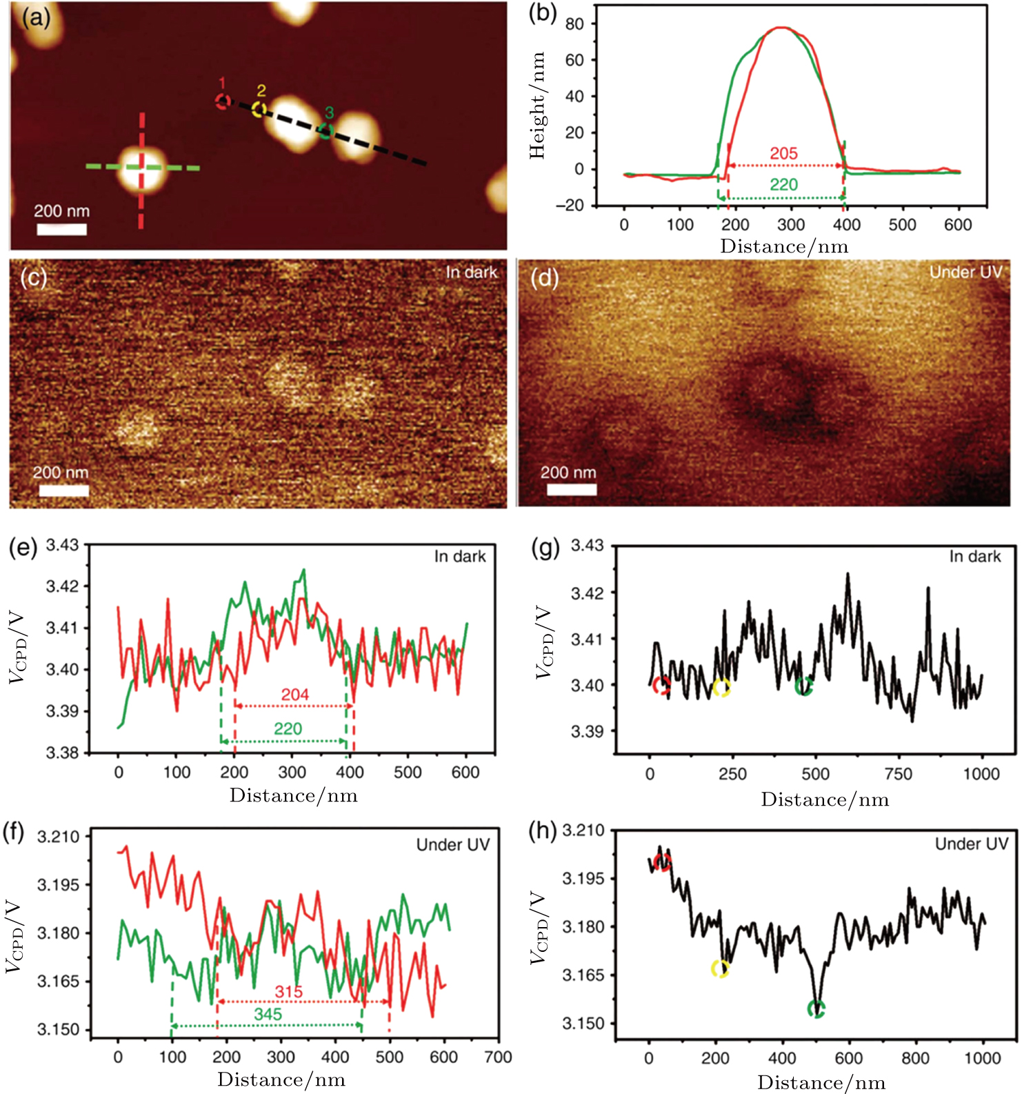
To reveal the physical mechanism, Kelvin probe force microscopy (KPFM) was adopted and the localized field enhancement induced by the surface plasmon was directly observed, which was regarded as the main reason for the enhancement.[41] Under ultraviolet illumination, the localized field enhancement results in the photogenerated electrons drifting close to the Ag NPs, and thus reducing the surface potential around the Ag NPs on the GaN epilayer as illustrated in Fig.
Based on this measurement, the physical mechanism for the responsivity enhancement of GaN UV detector utilizing Ag NPs was investigated in theory. The plots of polarizability versus energy for different sized nanospheres in a vacuum dielectric environment are shown in Fig.
 | Fig. 6. (color online) Surface potential reduction in the vicinity of Ag NPs on a GaN epilayer measured by Kelvin probe force microscopy (KPFM),[41] reproduced with copyright permission. |
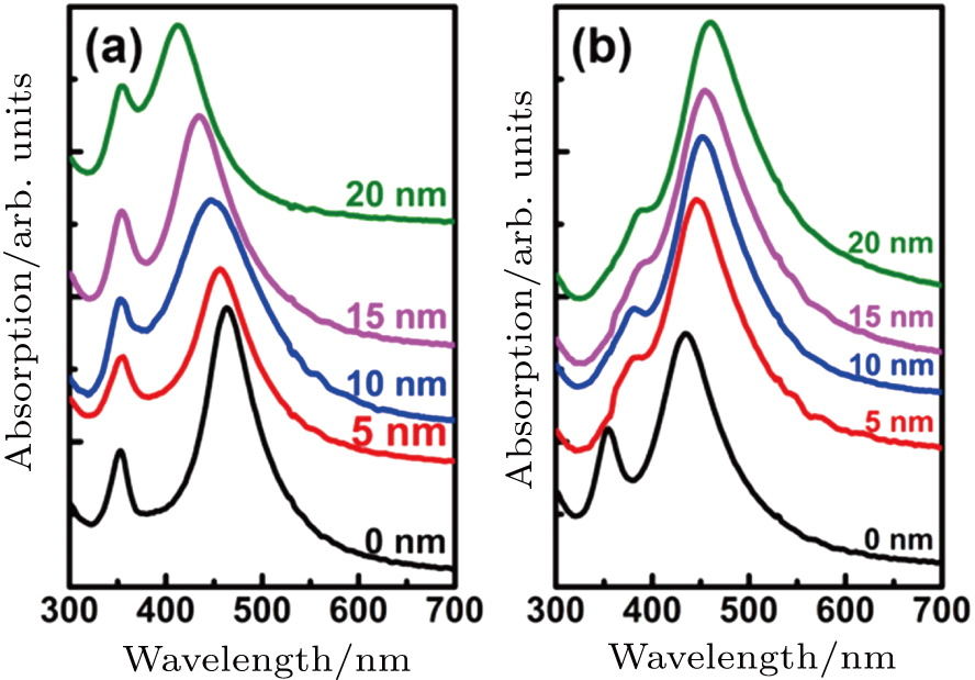
In order to achieve more effective resonant coupling, SiO2/Ag/SiO2 sandwich structures were studied by our team to render resonance wavelength more controllable.[42] The Ag/SiO2 structure was first fabricated, and the dipole surface plasmon resonance shifted from 470 nm to 410 nm by adjusting the SiO2 thickness beneath the Ag NPs from 5 nm to 20 nm. For SiO2/Ag/10 nm SiO2 sandwich structure, when changing the coating SiO2 thicknesses from 5 nm to 20 nm, the dipole surface plasmon resonance changed from 450 nm to 490 nm. This method can render the resonance peak position more controllable.
 | Fig. 7. (color online) (a) Plots of polarizability versus energy for a nanospheroid of different sizes, and (b) enhancement in the absorption rate with and without a spherical nanoparticle obtained in the quasi-static approximation. In both cases, the dielectric environment is vacuum.[41] All the above were reproduced with copyright permission. |
 | Fig. 8. (color online) Extinction spectra for (a) different SiO2 thickness beneath nanoparticles, ranging from 0 nm to 20 nm, (b) various thickness of SiO2 overcoating the NPs, ranging from 5 nm to 20 nm,[42] reproduced with copyright permission. |
Ag NPs also have significant enhancement for ZnO-based UV detector. The ZnO/Si MSM photodetector with Ag nanodisks on the top enhanced photocurrent by 30 times in 2016.[43] Kewei Liu et al. proposed and demonstrated Ag nanoparticles-decorated ZnO photodetectors for UV light sensing which can reduce dark current and increase peak responsivity at around 380 nm.[44] The device structure diagram and responsivity spectrum are shown in Fig.
The above method of preparing the Ag NPs is to evaporate Ag film first, and the metal film is then shrunk into Ag NPs by rapid thermal annealing (RTA) in N2 atmosphere. Actually, Ag NPs can also be synthesized by chemical methods. Zhang et al. obtained ZnO-based UV detectors with Ag plasmon fabricated by spin-coating the silver nanoparticle solution on ZnO films.[45] The responsivity increased more than 100 times, from 472 mA/W to 51.3 A/W because of the enhancement of Ag SPPs. In 2016, they adopted a sandwich structure of ZnO/AgNPs/ZnO to achieve a 22.3-times responsivity enhancement at a wavelength of 380 nm.[46]
 | Fig. 9. (color online) Device structure diagram and responsivity spectrum of ZnO photodetector with and without Ag NPs,[44] reproduced with copyright permission. |
In summary, Ag nanostructures have a significant enhancement in the performance of photodetectors in the near-UV wavelength range. However, Ag is not suitable in the short-wave UV region.
Aluminium (Al) is a highly promising material for commercial applications and it has the advantages of low price, high natural abundance and strong plasmon resonance. A dense oxide film was formed in the air rapidly, serving as a natural protective layer.[47] More importantly, the Al surface plasmon resonance wavelength has an absolute advantage in the short-wave UV region because Al has higher free electrons density. The bulk plasmon frequency is related to free electrons by
 |

Self-assembled Al nanostructure obtained through optimizing metal evaporation technique is studied for its advantages of simple operation and large area preparation. However, because of the high adhesion coefficient and good oxidability, it is difficult to fabricate Al nanoparticles by vacuum evaporation and rapid thermal annealing (RTA) process. This problem was solved by annealing the samples in-vacuum in the deposition chamber.[48] The Al film was evaporated onto the substrates at a temperature of 200 °C–400 °C, and then the annealing process was maintained in a vacuum for 60 min. The average size of particles depends on the thickness of the Al film as illustrated in Fig.
 | Fig. 10. SEM images in normal view (top row) and 60° tilted view (bottom row), showing average size of particles for film thickness of ((a), (d)) 7 nm, ((b), (e)) 14 nm, and ((c), (f)) 20 nm,[48] reproduced with copyright permission. |
 | Fig. 11. (color online) Schematic illustration of the method to obtain Al-NPs. (a) Comparison between thin films evaporated on substrate without (left panel) and with (right panel) a super-repellent surface functionalization. Scale bars on the SEM micrographs are 100 nm, and (b) detailed fabrication steps,[49] reproduced with copyright permission. |
Functionalized pre-processed substrate was realized by Martin et al, which can dramatically reduce the adhesion of Al to substrates.[49] After the functionalization, a super-repellent substrate was obtained. When thermally evaporated followed by 10-min-RTA at 800 °C, quasi-spherical Al nanoparticles with relatively homogeneous sizes were formed as illustrated in Fig.
In 2014, our team used angled electron beam evaporation to directly obtain Al nanoparticles on AlGaN epilayer and then realized the surface plasmon enhanced AlGaN deep UV detectors.[50] The size of Al NPs can be adjusted by changing the evaporation time as shown in Fig
 | Fig. 12. (color online) (a) Schematic illustration of Al NPs on AlGaN-based deep-UV detector. (b)–(d) SEM images of Al NPs with diameters of 20 nm, 40 nm, and 60 nm, respectively, deposited on the detectors, (e)–(f) two-dimensional (2D) morphology and corresponding cross-sectional profile of the Al NPs.[50] All the above were reproduced with copyright permission. |
In order to obtain more uniform Al nanostructures, one tried to make nanopatterns by using electron beam lithography (EBL), and then depositing metal to form nanostructures.[51] Figure
 | Fig. 13. (color online) (a) Schematic illustration of Al NPs-induced field enhancement on AlGaN-based deep-UV detector, and (b) spectral response of AlGaN detectors with and without Al NPs under a 5-V bias,[50] reproduced with copyright permission. |
 | Fig. 14. (color online) Main steps of EBL for depositing metallic nanostructures,[52] reproduced with copyright permission. |
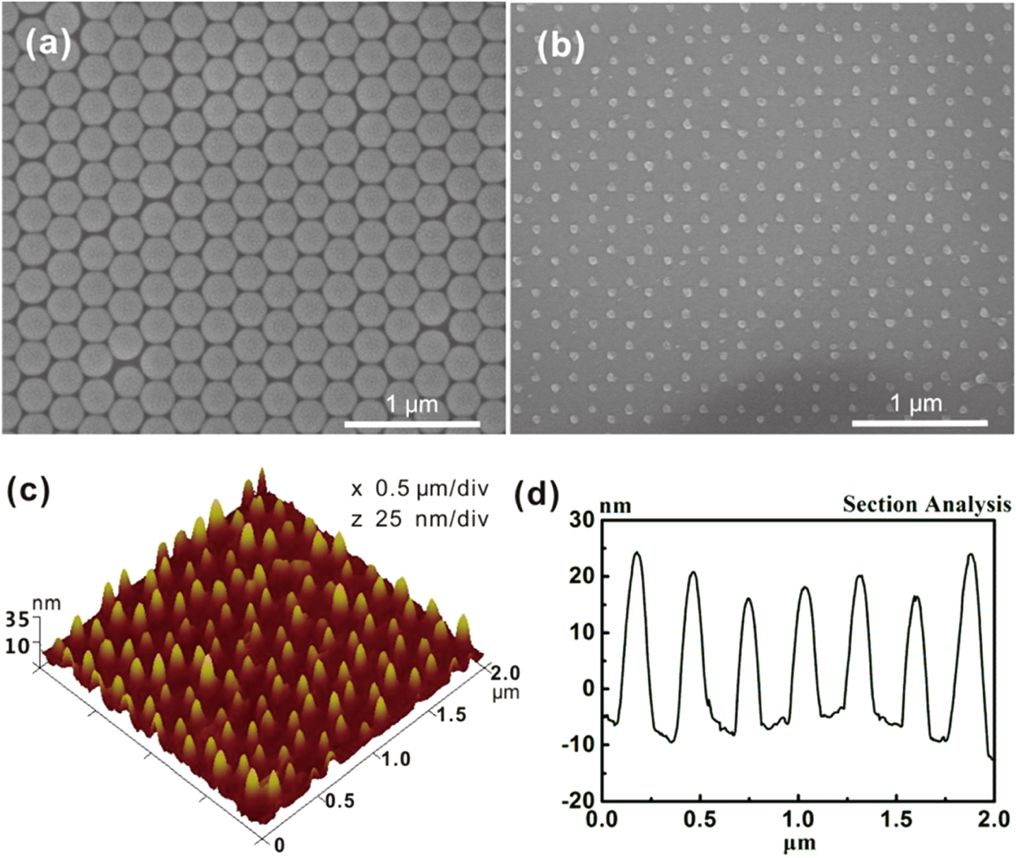
Nanosphere lithography (NSL) was considered to be an effective way to prepare Al nanoparticles array.[53–55] The NSL is based on the self-organization of colloidal particles such as polystyrene beads and transfer them onto surfaces to form 2D or three-dimensional (3D) evaporation masks,[56] and then metal was evaporated on the colloidal particles masks to form Al NPs. The nanostructures obtained by this method are in the form of triangle and can form relatively regular Al NPs arrays as shown in Fig.
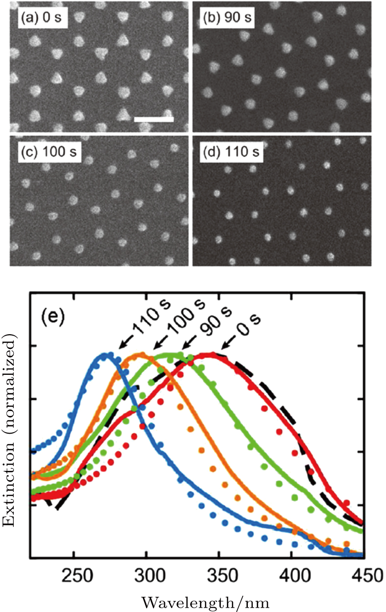
Obviously, the size of the metal nanostructure is completely determined by the diameter of the nanosphere mask, which limits the application range of this method. In order to fabricate Al NPs with different sizes by the NSL, a method was proposed to tune the space between the nanosphere masks.[57] Heating the nano-mask by using a microwave will result in the shrinking of the gap between them as illustrated in Fig.
 | Fig. 15. (color online) (a) SEM image of (a) as-prepared PS nanosphere monolayer and (b) fabricated Al nanoparticle arrays on AlGaN epilayer. (c) 3D morphology and (d) corresponding cross-sectional profile of the Al nanoparticle arrays obtained by AFM measurement.[31] All the above were reproduced with copyright permission. |
 | Fig. 16. (color online) (a) Dark current and photocurrent characteristic curves of the AlGaN-based MSM PDs with and without Al nanoparticles. (b) Spectral response of AlGaN-based MSM detectors with and without Al nanoparticles under 20-V applied bias. The inset shows the schematic illustration of the device with size-controlled and well-ordered Al nanoparticle arrays.[31] All the above were reproduced with copyright permission. |
 | Fig. 17. (color online) SEM images of Al nanostructures fabricated by using nanosphere masks heated for (a) 0 s, (b) 90 s, (c) 100 s, and (d) 110 s. The deposition thickness is 30 nm. The scale bar is 300 nm. (e) Normalized extinction spectra from the corresponding nanostructures.[57] All the above were reproduced with copyright permission. |
However, it is difficult to ensure the repeatability of Al NPs by the NSL method. Actually, such methods of coating involve a complex dynamic process associated with the evaporation of the colloidal solution influenced by the solvent type, concentration of the colloidal solution, volume spread onto the substrate, rotation speed, etc. More importantly, the size of the metal nanostructures is completely determined by the diameter of the colloids mask. In summary, this method has the merits of high-performance and low-cost but not suitable for large-area devices and cannot be applied to commercial production.
Al nanostructure has also been confirmed to be able to improve the performance of emerging ultra-wide band gap semiconductor photodetector.[58] The Al crescent-shaped arrays by nanosphere photolithography fabrication have been applied to diamond solar-blind UV photodetectors in 2016 by Zeng et al. The responsivity spectrum at 225 nm is about 28 mA/W at 5-V bias, which is over 10-fold more than that of the bare diamond detector. The results of this research also confirmed the absolute superiority of Al in short-wave UV.
In short, Al is a very promising material for plasmon in the UV region, especially in the deep UV region. However, there are still some problems in preparing the controllable Al nanoparticles and the mechanism of Al nanoplasmon enhancing the performance of deep UV detector needs to be further understood.
The wide band gap semiconductor UV photodetector has attracted much attention due to its excellent properties. Numerous efforts have been devoted to the detectors, but their performances are still far from the expectation. Surface plasmon provides a new way to improve the performance of UV photodetector. In this review, we present the fundamental of nanoplasmon and the recent experimental progress of surface plasmon applications in UV photodetectors. Table
| Table 1. Remarkable achievements of surface plasmon enhanced UV detectors. . |
In this paper, we mainly review the improvement of the spectral response of semiconductor UV photodetectors by metal nanoparticles surface plasmon effect. Ag NP can significantly enhance the performance of near-UV detector, while Al has an absolute advantage in the deep UV region. The metal type, size, density or distribution should be optimized to match the resonance of surface plasmon. In this case, the performance of wide band gap semiconductor based UV or deep UV detector will be enhanced. On the one hand, the mechanism of surface plasmon needs to be further understood in the future. On the other hand, the controllability and high repeatability of nanostructure should be prepared to realize the high performance detectors. In a word, the surface plasmon-enhanced ultraviolet photodetectors are promising and deserve to be further studied.
| [1] | |
| [2] | |
| [3] | |
| [4] | |
| [5] | |
| [6] | |
| [7] | |
| [8] | |
| [9] | |
| [10] | |
| [11] | |
| [12] | |
| [13] | |
| [14] | |
| [15] | |
| [16] | |
| [17] | |
| [18] | |
| [19] | |
| [20] | |
| [21] | |
| [22] | |
| [23] | |
| [24] | |
| [25] | |
| [26] | |
| [27] | |
| [28] | |
| [29] | |
| [30] | |
| [31] | |
| [32] | |
| [33] | |
| [34] | |
| [35] | |
| [36] | |
| [37] | |
| [38] | |
| [39] | |
| [40] | |
| [41] | |
| [42] | |
| [43] | |
| [44] | |
| [45] | |
| [46] | |
| [47] | |
| [48] | |
| [49] | |
| [50] | |
| [51] | |
| [52] | |
| [53] | |
| [54] | |
| [55] | |
| [56] | |
| [57] | |
| [58] |

