Efficiency-enhanced AlGaInP light-emitting diodes using transparent plasmonic silver nanowires*

Project supported by the National Key Research and Development Program of China (Grant No. 2016YFB0400603) and the National Natural Science Foundation of China (Grant No. 61335004).

Guo Xia1, †, Liu Qiao-Li2, Tian Hui-Jun2, Guo Chun-Wei2, Li Chong2, Hu An-Qi1, He Xiao-Ying1, Wu Hua3, ‡
School of Electronic Engineering, State Key Laboratory of Information Photonics and Optical Communications, Beijing University of Posts and Telecommunications, Beijing 100876, China
School of Electronic Information and Control Engineering, Beijing University of Technology, Beijing 100124, China
College of Physics and Electronic Information, Gannan Normal University, Ganzhou 341000, China


† Corresponding author. E-mail: guox@bupt.edu.cn wh1125@126.com

Project supported by the National Key Research and Development Program of China (Grant No. 2016YFB0400603) and the National Natural Science Foundation of China (Grant No. 61335004).

Abstract

Silver nanowire (AgNW) networks have been demonstrated to exhibit superior transparent and conductive performance over that of indium-doped tin oxide (ITO) and have been proposed to replace ITO, which is currently widely used in optoelectronic devices despite the scarcity of indium on Earth. In this paper, the current spreading and enhanced transmittance induced by AgNWs, which are two important factors influencing the light output power, were analyzed. The enhanced transmittance was studied by finite-difference time-domain simulation and verified by cathodoluminescence measurements. The enhancement ratio of the light output power decreased as the GaP layer thickness increased, with enhancement ratio values of 79%, 52%, and 15% for GaP layer thicknesses of 0.5 μm, 1 μm, and 8 μm, respectively, when an AgNW network was included in AlGaInP light-emitting diodes. This was because of the decreased current distribution tunability of the AgNW network with the increase of the GaP layer thickness. The large enhancement of the light output power was caused by the AgNWs increasing carrier spread out of the electrode and the enhanced transmittance induced by the plasmonic AgNWs. Further decreasing the sheet resistance of AgNW networks could raise their light output power enhancement ratio.

1. Introduction

AlGaInP light-emitting diodes (LEDs) are widely applied in traffic signals and backlighting units for liquid crystal displays.[1,2] Indium-doped tin oxide (ITO) is commonly used as the transparent conductive layer on the top of LED structures to spread the carriers away from the opaque electrodes to enhance the quantum efficiency and avoid current crowding under the electrodes.[3] However, the scarcity of indium on Earth is causing the price of ITO to soar, thus raising the cost of LED chips.[4,5] Recently, commercially percolated silver nanowire (AgNW) networks have received much attention because they demonstrate promising transparent conductive performance originating from their low inter-wire junction resistance and low absorption loss.[6] The transmittance and sheet resistance of AgNW networks, which are two figures of merit to evaluate transparent conductive performance, reached ∼ 93.5% at 550 nm and ∼ 21.1 Ω/sq, respectively, when used as a skin-like pressure sensor.[7] A purified AgNW film could further improve the transmittance to 97.5% while keeping the sheet resistance below 70 Ω/sq.[8] AgNW networks can improve the optical performance when applied to optoelectronic devices. For example, the external quantum efficiency of AlGaInP LEDs was improved by 80%–100% when an AgNW network was used as a transparent conductive layer.[9,10] The efficiency of an organic solar cell containing an AgNW network electrode was demonstrated to be 1.45 times higher than that using an ITO electrode.[11] The efficiency enhancement was attributed to the current spreading and the charge injection. The electrical and optical performances of LEDs are interrelated. However, the joint electrical and optical effects of AgNW networks on the light output power of LEDs have not yet been studied. There is still much research that needs to be conducted before ITO can be replaced with AgNW networks in commercial optoelectronic devices, such as LEDs.

In this paper, the mechanism of the optical transmittance enhancement of AgNWs induced by surface plasmons (SPs), which is one of the important factors affecting the light output power of LEDs, is studied in detail. For AlGaInP LEDs with GaP layer thicknesses of 0.5 μm, 1 μm, and 8 μm, the maximum light output power increases by about 79%, 52%, and 15%, respectively, upon substitution of ITO with AgNWs. We examine the reason why the enhancement ratio of the light output power of AlGaInP LEDs decreases with the increase of the GaP thickness.

2. Experiments and results

AlGaInP LEDs were grown on n-GaAs substrates by metal–organic chemical vapor deposition. Fifteen pairs of Al0.6Ga0.4As/AlAs layers with distributed Bragg reflectors were grown on a 100-nm-thick GaAs buffer layer. The active region was composed of 800-nm-thick 60-period (Al0.5Ga0.5)0.5In0.5P/(Al0.1Ga0.9)0.5In0.5P multiple quantum wells (MQWs), which were sandwiched in p- and n-(Al0.7Ga0.3)0.5In0.5P cladding layers for electron and hole confinement. To study the current spreading effect of the AgNW network, three thicknesses of the Mg-doped p-GaP window layer were used in this work, which were 0.5 μm, 1 μm, and 8 μm, with a doping density of 5 × 1018 cm−3. Au (50 nm)/BeAu (150 nm)/Au (200 nm) with a diameter of 100 μm was first deposited and then patterned by wet etching as the p-type electrode. After the LED wafer was lapped down to around 200 μm, AuGeNi (50 nm)/Au (300 nm) was deposited as the n-type electrode. The wafer was annealed in nitrogen at 430 °C for 30 s. Then AgNW solution with a concentration of 0.5 mg/mL or 1.5 mg/mL was spin coated at 270 rpm on the LED surface to provide a uniform distribution and then stuck on the LED surface through the van der Waals force. Each LED with an AgNW film was put on a hot plate at 200 °C for 10 min to lower the nanowirenanowire contact resistance. Each LED wafer was scribed into chips (300 μm × 300 μm), and then were packaged. The light output power and electroluminescent spectrum were carried out by integrating sphere (Ocean Optics USB 2000+), and the current–voltage (IV) curves were measured by Keithley 4200.

Figures 1(a) and 1(b) show scanning electron microscopy (SEM) images of AgNW films on Si substrates prepared by spin coating AgNW solutions with the concentrations of 0.5 mg/mL and 1.5 mg/mL, respectively. The insets display the corresponding magnified images. The typical diameter and length of the nanowires measured from the SEM images are about 40 nm and 30–50 μm, respectively. The average side length of the area not covered by AgNWs for the two samples is less than 1 μm and decreases with the increase of the AgNW solution concentration. 0.5 mg/mL and 1.5 mg/mL AgNW solutions are coated by spinning on the glass substrate to determine the transmittance (Shimadzu UV-VIS-NIR Spectrophotometer). Figure 1(c) shows the spectral transmittance measurement results from 300 nm to 800 nm. The transmittance curve generally decreases with the AgNW concentration because of the larger area covered by the opaque metal nanowires, as illustrated by the SEM images in Figs. 1(a) and 1(b).[9,10] The decrease in the transmittance curves between 300 nm and 400 nm is caused by the absorption of SPs.[11,12] The optical transmittance at 550 nm (T550nm) is 94.3% and 82.4% for AgNW networks formed using solution concentrations of 0.5 mg/mL and 1.5 mg/mL, respectively. The corresponding sheet resistance R is ∼ 20 Ω/sq and 7.2 Ω/sq, respectively, which are measured by the four-probe method. These values match well in terms of their TR balance.[9,13]

Fig. 1. (color online) SEM images of AgNW networks formed on Si substrates by spin coating with AgNW solution concentrations of (a) 0.5 mg/mL and (b) 1.5 mg/mL. The insets are the corresponding magnified images at a magnification of 5 × 10⁴. (c) Spectral transmittance of AgNW networks on glass substrates prepared by spin coating at 270 rpm using AgNW concentrations of 0.5 mg/mL and 1.5 mg/mL.

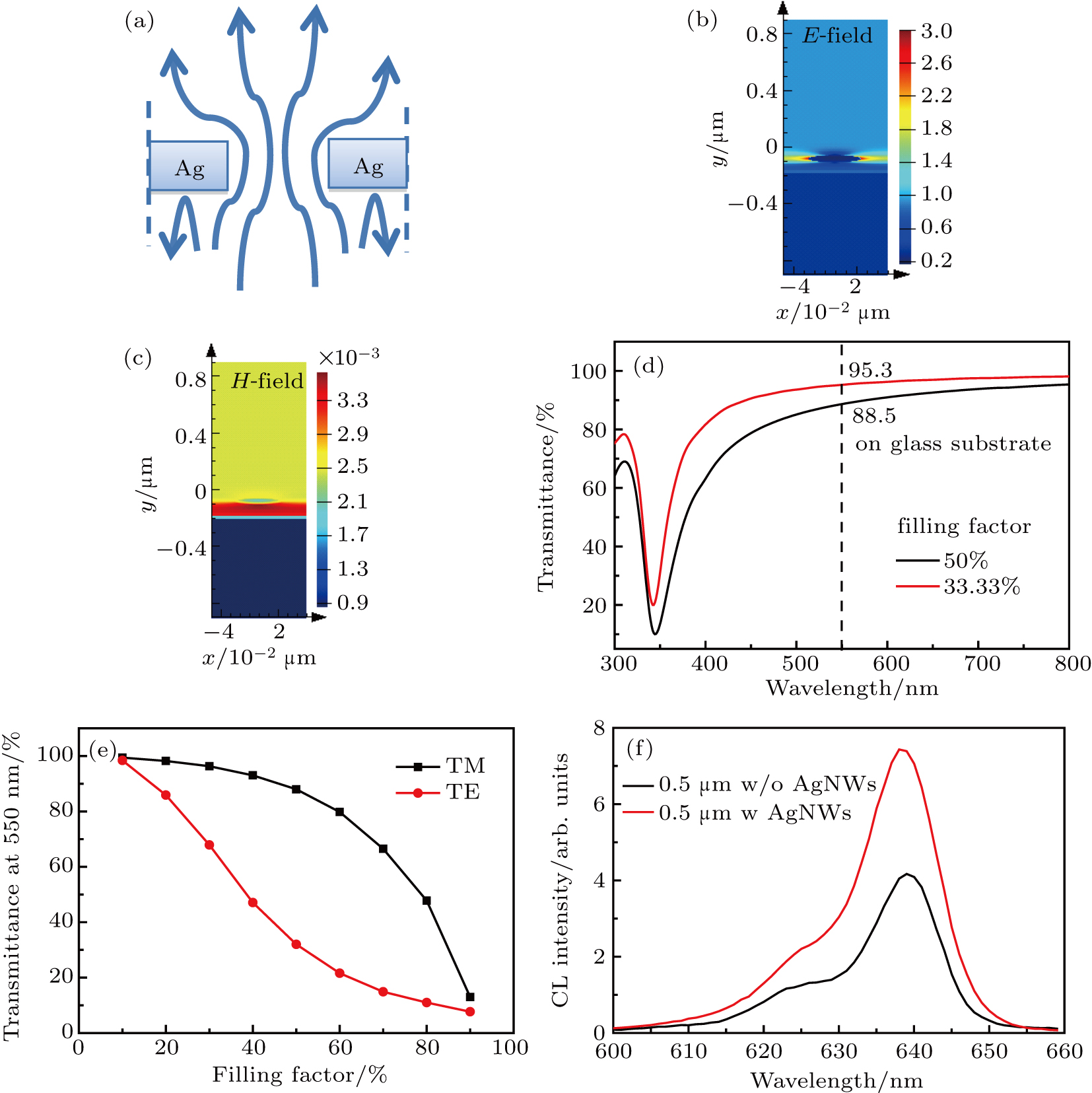
The high transmittance of the AgNW network, because of the absorption behavior of Ag, could be considered to originate from the exposed area. We count the number of Ag-NWs in the SEM images in Figs. 1(a) and 1(b), and then estimate the coverage area according to the specific dimensions of nanowires also measured from the SEM images. Without considering the overlap area of the AgNWs, the coverage ratio is about 1/3 and 1/2 for the AgNW solution concentrations of 0.5 mg/mL and 1.5 mg/mL, respectively. Intuition tells us that the opaque metal wires will block the geometric light path; accordingly, the maximum optical transmittance is predicted to be 66.7% and 50%, respectively. The obvious enhancement of both optical and microwave transmission, where the subwavelength-sized exposed area transmits more electromagnetic waves than predicted by geometrical optics, has been observed in many experiments.[11,12] Figure 2(a) shows a conceptual drawing of the extra light transmission through the subwavelength openings. The electromagnetic wave could bypass the obstacles.

Fig. 2. (color online) FDTD simulation results of enhanced transmission through periodic AgNW openings. (a) Conceptual drawing of the extra light transmission through a subwavelength opening. (b) and (c) FDTD simulation results of electric and magnetic field distribution of a one-period structure by a normal incident TM polarized plane wave at 550 nm. The AgNW filling factor is 50% on a glass substrate with a period of 100 nm. (d) Calculated transmittance from 300 nm to 800 nm with AgNW filling factors of 33.33% and 50% on glass substrates with normal-incidence TM polarized plane waves. (e) The dependence of transmittance at 550 nm on the AgNW filling factor for TE and TM polarized plane waves. (f) Cathodoluminescence measurement results for AlGaInP LEDs with and without an AgNW network fabricated using a solution concentration of 0.5 mg/mL.

To ensure accurate analysis of the light transmission, the electric and magnetic field distribution of a one-period AgNW structure by a normal incident transverse magnetic (TM) polarized plane wave at 550 nm is calculated by finite-difference time-domain (FDTD) simulation for an AgNW filling factor of 50% on a glass substrate, as presented in Figs. 2(b) and 2(c). The period is set to 100 nm. As expected, the incident light is coupled by such metal network. The transversal dipolar plasmonic resonance occurs around the AgNWs and decreases quickly with lengthening distance from the AgNW/glass interface, which is called local surface plasmonic resonance.[14,15] Surface plasmons are surface waves with electromagnetic fields confined to the vicinity of the metal–dielectric interface. When the resonance condition is fulfilled, this confinement leads to enhancement of the electromagnetic field at the AgNW interface because of the low imaginary part of its refractive index. The transmittance in this region can increase substantially because of the enhancement of the local electromagnetic field. Figure 2(c) shows the curves of transmission versus the wavelength calculated by FDTD simulation for filling factors of 33.33% and 50%. The predicted behavior is the same as that observed experimentally, as shown in Fig. 1(d). The plasmonic resonance occurs below 400 nm and then the high transmittance is relatively stable at wavelengths longer than 500 nm. The calculated T550nm is 95.3% and 88.5% for the AgNW filling factors of 33.33% and 50%, respectively, which coincides well with the experimental results. Figure 2(e) plots the dependence of the transmittance at 550 nm on the AgNW filling factor. For TM polarization, the incident angle is perpendicular to the surface and then perpendicular to the long axis of the AgNW. The transmittance decreases from 100% to zero as the filling factor increases because the exposed area for light transmission decreases. The transmittance of TM polarization is always larger than that of transverse electric (TE) polarization, whose light polarization is parallel with the long axis of AgNWs. The TE and TM resonance modes decrease to a relatively low level with further increase of the filling factor, as shown in Fig. 2(e), because the SPs could not be sufficiently excited, which confirms that the transmittance enhancement by the AgNW network is caused by the TM polarized incident plane wave, which excites considerable electromagnetic resonance.

Cathodoluminescence (CL) measurements were carried out to confirm the plasmonic transmittance enhancement of the AgNW network. The carriers in the MQWs were uniform, which were excited by a continuous wave (CW) electron beam (e-beam).[16] The measurement system was a spatially resolved CL spectroscope (Gatan Mono 3+) combined with a field-emission environmental scanning electron microscope (ESEM). The ESEM-CL system allowed the observation and measurement of nanostructures with a spatial resolution of 1.2 nm and spectral precision of 0.66 nm. The experimental conditions of the ESEM and the CL spectrometer included an accelerating voltage of 20 kV, an e-beam current of 0.1 nA to 10 nA, a working distance of 12.6 mm, and a photomultiplier tube (PMT) detector with a grating of 1200 l/mm. The detection wavelength of the PMT detector ranged between 200 nm and 930 nm. Figure 2(f) depicts the CL measurement results for the AlGaInP LEDs with and without an AgNW network formed using a solution concentration of 0.5 mg/mL from 600 nm to 660 nm. The wavelength peak is located at 639 nm, which coincides with the electroluminescence spectrum of the LED. The CL power ratio of the LEDs with and without AgNWs is about 1.8. Because non-uniform carrier distribution is avoided in the MQWs, the 80% additional enhancement of CL power is caused by the plasmonic effect of the AgNWs, which could enhance the device transmittance.

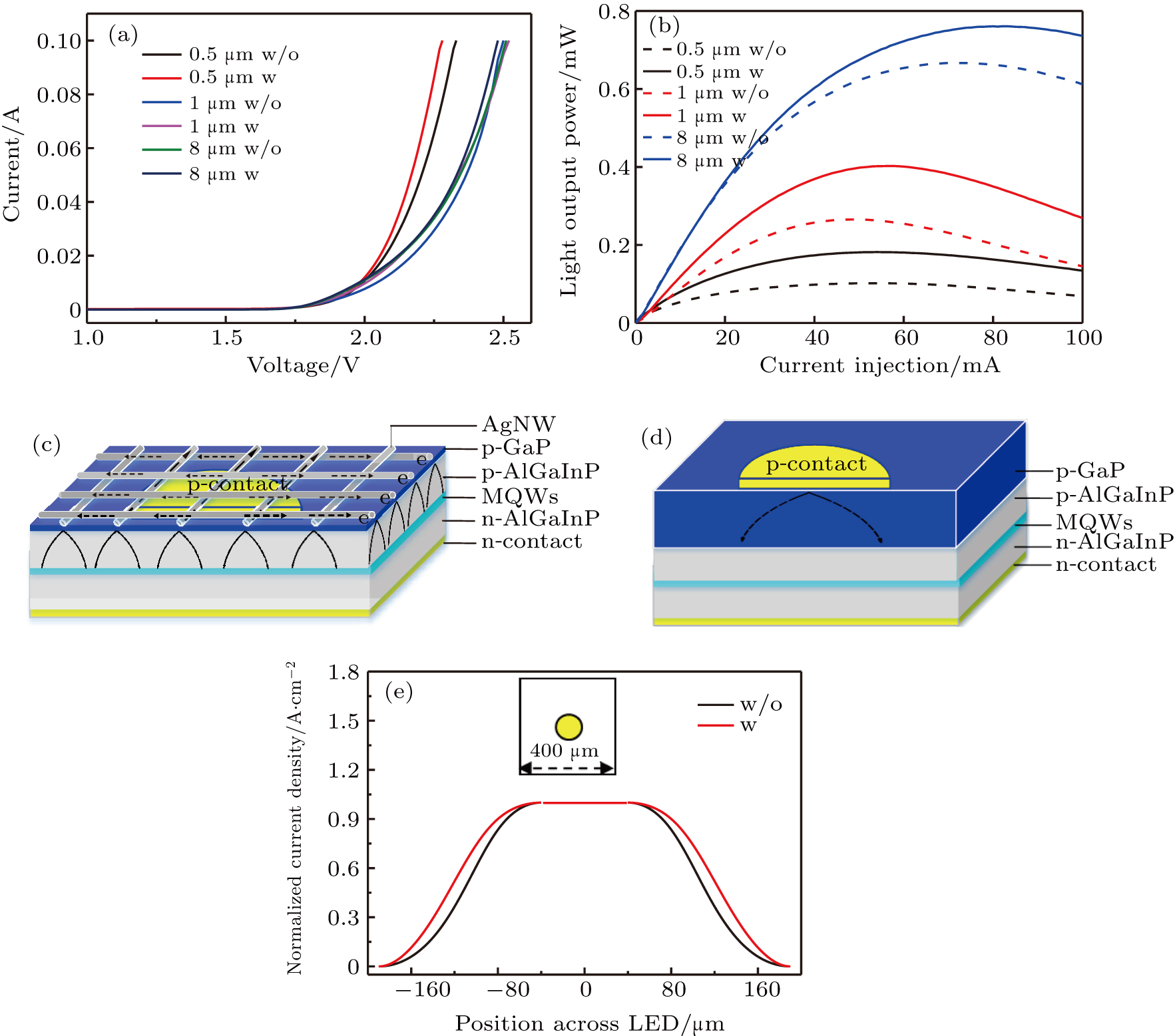
Figure 3(a) presents the IV measurements for LEDs with and without AgNW networks and GaP layer thicknesses of 0.5 μm, 1 μm, and 8 μm. The AgNW concentration is 0.5 mg/mL because it gives a better figure of merit as a transparent conduction layer in our experiments than a concentration of 1.5 mg/mL. The voltage drop decreases a little after applying AgNWs because of the decrease of lateral resistance, with values of 2.07 V, 2.12 V, and 2.12 V at 20 mA for the LEDs with GaP layer thicknesses of 0.5 μm, 1 μm, and 8 μm, respectively. Figure 3(b) compares the light output power versus dc current injection behavior of AlGaInP LEDs with and without AgNW networks on their surface at room temperature. Before applying the AgNW network, the maximum light output powers for the AlGaInP LEDs with GaP layer thicknesses of 0.5 μm, 1 μm, and 8 μm at 20 mA are 0.1019 mW, 0.2657 mW, and 0.6668 mW, respectively, because of the better current spreading in the LED with a thicker GaP layer. After applying the AgNW network, the maximum light output powers increase to 0.1818 mW, 0.4025 mW, and 0.761 mW for the AlGaInP LEDs with GaP layer thicknesses of 0.5 μm, 1 μm, and 8 μm, respectively; thus, the light output power increases by about 79%, 52%, and 15%, respectively. The increase of the output power decreases with the increase of the GaP layer thickness.

Fig. 3. (color online) Electrical and optical characteristics of AlGaInP LEDs with AgNW networks fabricated using a solution concentration of 0.5 mg/mL. The top GaP window layer thickness was 0.5 μm, 1 μm, or 8 μm. (a) Current–voltage measurements for AlGaInP LEDs with and without AgNW networks. (b) Comparison of the light output powers of AlGaInP LEDs with and without an AgNW network versus dc injection at room temperature. Current injection modes of the AlGaInP LEDs (c) with and (d) without AgNW networks. (e) Calculated normalized current density distribution inside the GaP window layer for square AlGaInP LED chips with and without an AgNW network on the surface of GaP.

The enhancement of transmittance induced by the SPs of AgNWs should be the same for all the samples with different GaP layer thicknesses, which indicates that the increase of the light output power should also be the same. However, the electrical properties of the AgNW network and GaP window layer determine the current distribution as well as the light emission profile of the LEDs. Figures 3(c) and 3(d) provide schematics of the AlGaInP LEDs with AgNW networks and different GaP layers. For the conventional LEDs with only a GaP layer, the current will spread laterally in the GaP window layer, as determined by the lateral electric field inside the LEDs. The lateral current spreading length increases with the GaP layer thickness according to LS = [(ρc + ρGaPtGaP)tn/ρn]1/2, where LS is denoted as the current spreading length, over which the current density drops to the 1/e value of the current density at the edge, ρc is the p-type specific contact resistance, ρGaP is the resistivity of the p-type GaP layer, ρn is the resistivity of the n-type layer, and tGaP and tn are the thicknesses of the GaP and epitaxial layers, respectively.[17] Limited by the mobility of holes, carriers are crowded under the electrode and then lots of the light is blocked by the opaque electrode in conventional LEDs with a thin GaP layer.[2,18] When AgNWs are included on the LED surface, the current can be spread with the aid of the metal nanowires, which can increase LS. Then, the nanowires behave as many mini injectors, injecting the current into the LEDs for lighting. That is the reason for the enhancement of the light output power when an AgNW network is included in the LEDs. The improvement ratio of the light output power is determined by the parallel resistance of the GaP layer and AgNW network. LS under the aid of AgNWs depends on the ratio of the sheet resistance between the AgNW network and GaP layer, which are connected in parallel. According to its doping density and thickness, the calculated sheet resistance of the GaP layers is about 200 Ω/sq, 100 Ω/sq, and 12 Ω/sq for GaP layer thicknesses of 0.5 μm, 1 μm, and 8 μm, respectively, according to ρ = 1/(neμ) and sheet resistance R/t = ρ/S, in which ρ is the electrical resistivity, n is the carrier density, e is the elementary charge, μ is the mobility, R is the resistance, t is the thickness of p-type GaP, and S is the LED chip area. Compared with the sheet resistance R of 20 Ω/sq for the AgNW network, that of the GaP layer decreases with the increase of the layer thickness until it is smaller than that of the AgNW network, which indicates that the dominant current spreading path changes from the AgNW film to the GaP layer at this point. That is, for the LED with a GaP layer thickness of 0.5 μm, most of the current is spread by AgNWs and then injected into the GaP layer by the nanowires, as illustrated in Fig. 3(c). Meanwhile, for the LED with a GaP thickness of 8 μm in Fig. 3(d), the lateral current is spread mainly through the GaP layer directly, not the AgNWs. Figure 3(e) shows the effect of the presence of an AgNW network on the GaP window layer, simulated by Silvaco. The normalized current intensity is plotted as a function of the lateral position of the AlGaInP LED chip with a 60-μm-thick GaP current-spreading layer. A GaP layer thickness of 60 μm means the current can spread throughout the whole quantum well area of the LED.[18] As shown in Fig. 3(e), current density keeps constant under the electrode for both LEDs. Carrier will spread out of the electrode under the action of electric field. For both types of LED, current density decreases exponentially when the position is outside the electrode due to the lateral resistance of GaP or AgNW network. Due to the AgNW involved, LS increases from 42.2 μm to 73.8 μm according to the fitting results. The voltage drop increases with the resistance of current spreading layer at the position outside the electrode as well, which coincides with the current density dropping profile. However, improved current spreading decreases with the GaP layer thickness, due to the competition between the sheet resistance of AgNW network and GaP.

Light generated outside the electrode can be enhanced by the plasmonic AgNWs, which indicates that the more the current spreads out, the more the light transmittance is enhanced. For the LED with a 0.5-μm-thick GaP layer, the highest increase ratio of light output power of 79% is mainly attributed to the increased lateral current spreading and then the plasma-enhanced transmittance. Meanwhile, for the LED with an 8-μm-thick GaP layer, the enhancement of light output power by the AgNWs is the smallest among all the LEDs. This is because the AgNWs have little effect on the lateral current spreading in this case, so only a portion of the optical field outside the electrode on the LED surface has the chance to obtain the enhanced transmittance.

3. Conclusion and perspectives

The light output power of AlGaInP LEDs with AgNWs as a transparent conductive layer for current spreading was examined. It was found that the increase of the ratio of light output power of AlGaInP LEDs with and without AgNWs decreased with the increase of GaP layer thickness, which was attributed to the decreased tunability of the additional current spreading caused by the AgNW network. When the sheet resistance of the GaP layer was lower than that of AgNW networks, which are connected in parallel, the current spreading path changed from AgNWs to GaP. The output light increase of about 79% obtained for the thin GaP layer was mainly attributed to the current spreading induced by the AgNWs and then their SP-enhanced transmittance effect. The optimized results show that large power enhancement and well contact can be obtained both by using this new technology, in which better carrier transportation and light transmittance are achieved at the same time.

Reference
[1] Huang K H Yu J G Kuo C P Fletcher R M Osentowski T D Stinson L J Liao A S H 1992 Appl. Phys. Lett. 61 1045
[2] Vanderwater D A Tan I H Hofler G E Defevere D C Kish F A 1997 Proc. IEEE 85 1752
[3] Hsu S C Wuu D S Lee C Y Su J Y Horng R H 2007 IEEE Photonic Tech. Lett. 19 492
[4] Kim B J Lee C M Jung Y H Baik K H Mastro M A Hite J K Eddy C R Kim J Y 2011 Appl. Phys. Lett. 99 143101
[5] Seo T H Lee K J Oh T S Lee Y S Jeong H Park A H Kim H Choi Y R Suh E K Cuong T V Pham V H Chung J S Kim E J 2011 Appl. Phys. Lett. 98 251114
[6] Kim J H Triambulo R E Park H W 2017 J. Appl. Phys. 121 105304
[7] Lee C J Jun S Ju B K Kim J W 2017 Phys. B: Condens. Matter 514 8
[8] Gebeyehu M B Chala T F Chang S Y Wu C M Lee J Y 2017 RSC Adv. 7 16139
[9] Guo X Guo C W Wang C Li C Sun X M 2014 Nanoscale Res. Lett. 9 670
[10] Im H G Jin J H Ko J H Lee J M Lee J Y Bae B S 2014 Nanoscale 6 711
[11] Liu X F Wu B Zhang Q Yip J N Yu G N Xiong Q H Mathews N Sum T C 2014 ACS Nano 8 10101
[12] Li W D Hu J Chou S Y 2011 Opt. Express. 19 21098
[13] Liu B Li C Liu Q L Dong J Guo C W Wu H Zhou H Y Fan X J Guo X Wang C Sun X M Jin Y H Li Q Q Fan S S 2015 Appl. Phys. Lett. 106 033101
[14] William L B Alain D Thomas W E 2003 Nature 424 824
[15] Ma Y Q Shao J H Zhang Y F Lu B R Zhang S C Sun Y Qu X P Chen Y F 2015 Chin. Phys. 24 080702
[16] Wang L Wang X D Mao S C Wu H Guo X Ji Y Han X D 2016 Nanoscale 8 4030
[17] Guo X Schubert E F 2001 Appl. Phys. Lett. 78 3337
[18] Chi G C Su Y K Jou M J Hung W C 1994 J. Appl. Phys. 76 2603