Project supported by the National Natural Science Foundation of China (Grant No. 51671098) and the Program for Changjiang Scholars and Innovative Research Team in University, China (Grant No. IRT16R35).
Project supported by the National Natural Science Foundation of China (Grant No. 51671098) and the Program for Changjiang Scholars and Innovative Research Team in University, China (Grant No. IRT16R35).
† Corresponding author. E-mail:
Project supported by the National Natural Science Foundation of China (Grant No. 51671098) and the Program for Changjiang Scholars and Innovative Research Team in University, China (Grant No. IRT16R35).
Magnetization manipulation by an electric field (E-field) in ferromagnetic/ferroelectric heterostructures has attracted increasing attention because of the potential applications in novel magnetoelectric devices and spintronic devices, due to the ultra-low power consumption of the process. In this review, we summarize the recent progress in E-field controlled magnetism in ferromagnetic/ferroelectric heterostructures with an emphasis on strain-mediated converse magnetoelectric coupling. Firstly, we briefly review the history, the underlying theory of the magnetoelectric coupling mechanism, and the current status of research. Secondly, we illustrate the competitive energy relationship and volatile magnetization switching under an E-field. We then discuss E-field modified ferroelastic domain states and recent progress in non-volatile manipulation of magnetic properties. Finally, we present the pure E-field controlled 180° in-plane magnetization reversal and both E-field and current modified 180° perpendicular magnetization reversal.
Magnetic tunnel junctions (MTJs) with an AlOx or MgO insulating barrier have been widely used in many fields, such as the read heads of hard disk drives (HDD), weak magnetic field detection, and sensitive magnetometers.[1–4] The essence of MTJs is the identification of parallel and anti-parallel magnetization of two ferromagnetic electrodes, with low-resistance and high-resistance states, respectively. This has been regarded as an outstanding example of the commercialization of scientific research.[5] At present, in both the cases of traditional HDD and the developing magnetic random access memory (MRAM), the question of writing magnetic information to represent “0” and “1”, i.e., the manipulation of the two distinguishable magnetization states in MTJs, is still a challenging issue with respect to an in-depth understanding of the physical mechanism involved and the realization of practical applications. In a traditional magnetic field based MRAM, the magnetization orientation of the free layer in the MTJs is controlled by magnetic fields produced by two orthogonal conducting lines. The approach is hindered by several technical bottlenecks, which include:[5,6] (i) the conducting lines occupy a significant amount of space and the broad magnetic field distribution could disturb the adjacent memory cell; and (ii) when the size of memory cells is decreased further to improve storage density, a high current density (∼107 A/cm2) is required. In recent years, based on the spin transfer torque (STT) effect[7–9] and spin–orbit torque (SOT) effect,[10–12] STT-MARM has entered a stage of industrialization,[13] and the SOT-MRAM has been realized in the laboratory.[14] However, they also face some technical difficulties, such as how to decrease the threshold current density (Jc) to about 105 A/cm2 and realize magnetization switching without the assistance of an in-plane magnetic field in SOT-MRAM.[15] In addition to the magnetic field and current induced relevant effects, light, strain, phase transition, and electric field (E-field) are also able to effectively regulate magnetism.[16–19] Among them, E-field control of magnetic properties not only is able to significantly decrease the Joule heating effect, but also can realize non-volatile, reversible, and high-density data storage with low power consumption.
Generally, in the area of E-field control of magnetism, candidate materials primarily include magnetic semiconductors,[20] ferromagnetic metals,[21] and multiferroic materials.[22] The propagation of domain walls (DWs) and the modification of magnetic properties are promising approaches for the realization of high-density magnetic memory and magnetic logic elements. Lei et al. demonstrated that DW motion can be electrically controlled through strain-mediated magnetoelectric coupling in piezoelectric/ferromagnetic nanostructures at room temperature, and that the energy barrier for DW motion can be doubled under reasonable electric fields.[23] Rushforth et al. demonstrated that voltage induced strain can effectively regulate magnetic anisotropy, anisotropic magnetoresistance, and nonvolatile switching of the magnetization direction in a (Ga,Mn)As device bonded to a piezoelectric transducer. Meanwhile, calculations based on the mean-field kinetic exchange model of (Ga,Mn)As facilitate a microscopic understanding of the measured effect.[24] Li et al. reported that the piezo voltages manipulate the magnetic properties of the Fe/n-GaAs/piezoelectric heterostructure. By measuring the magnetic hysteresis loops under the piezo voltages, the manipulation of two-jump to one jump magnetization switching can be realized. These findings could be very important for future metal-semiconductor spintronic applications.[25] In comparison, many investigations have focused on multiferroic materials combined with ferroelectricity, ferromagnetism, and ferroelasticity. The three ferroic order interactions can lead to diverse phenomena. For example, the ferroelectricity and ferroelasticity present the piezoelectric effect, ferromagnetism and ferroelasticity present the piezomagnetic effect, and ferroelectricity and ferromagnetism present the magnetoelectric (ME) effect. Magnetism could be manipulated by the converse ME coupling effect with an applied E-field, which is a promising method to fabricate energy-efficiency spintronic devices.[26–28] Single-phase multiferroic materials are rare and only present ME coupling effects well below room temperature.[29] BiFeO3 is a unique example of such a material that has already been proved to exhibit ferroelectricity and weak anti-ferromagnetism (AFM) at room temperature.[30] For artificial ferromagnetic/ferroelectric (FM/FE) heterostructures with coupling between the ferromagnetic layer with a high magnetostrictive effect and a ferroelectric layer with a large piezoelectric effect, the magnetic properties of the FM can be effectively adjusted by the converse ME coupling effect. The coupling mechanisms in such FM/FE heterostructures mainly include the charge mediated effect through charge accumulation/dissipation at the FM/FE interface, the exchange bias mediated effect resulting from the AFM properties of the FE layer, the strain mediated effect by means of transferring strain from the FE layer to the FM layer, as well as the emergent mechanisms of orbital reconstruction and the electrochemical effect in ultrathin films. It should be noted that the aforementioned coupling mechanisms may coexist, and the main features of the last one are highlighted in previous reviews.[27,31] Among them, the strain-mediated mechanism has received a lot of attention in recent years, because this method is particularly convenient and effective at room temperature. Moreover, the incorporation of FE materials is optional for this purpose, given the large piezoelectric coefficients and/or the piezoelectric memory effect. For example, BaTiO3,[32] Pb(Zr1−xTix)O3 (PZT),[33] [Pb(Mg1/3Nb2/3)O3]x-[PbTiO3]1−x (PMN-PT),[34] and [Pb(Zn1/3Nb2/3)O3]x-[PbTiO3]1−x (PZN-PT)[35] are usually used as FE layers in the FM/FE heterostructures. Alternative materials which exhibit magnetostriction effects that serve as FM layers can be widely chosen from the amorphous to single crystal phase, and from the magnetic isotropic to the magnetic anisotropic materials. So far, E-field induced strain-mediated orientation of magnetization, magnetic anisotropy, coercivity, and ferromagnetic resonance frequency have been realized in ferromagnetic/piezoelectric actuator hybrid structures or FM/FE heterostructures.[36–40]
In this context, we will review some exciting research on E-field control of magnetism by means of strain-mediated magnetoelectric coupling. In Section
Compared to the interface charge mediated effect, transferring the strain from FE to FM film usually leads to giant magnetic property modification in thick FM films. In normal (001) PMN-PT materials,[41] the E-field dependence on the in-plane strain (S–E) curve shows symmetric butterfly-like variation. After removing the applied E-field, the residual stress vanishes, i.e., the in-plane strain is volatile. When an isotropic magnetic films is fabricated on the (001) PMN-PT substrate, its volatile magnetic response shows a similar behavior to the S–E curve. In CoFe2O4/(001) PMN-PT heterostructure,[42] as shown in Figs.
 | Fig. 1. (color online) (a) In-plane ΔM/M(0)–E loop, the magnetic field is 0.05 T. (b) Out-of-plane. ΔM/M(0)–E loop, the magnetic field is 0.2 T (from Fig. |
For the amorphous or polycrystalline FM films with UMA, the hysteresis loop (M–H) along the EA direction is square, whereas the hysteresis loop along the hard axis (HA) direction is slanted with a fairly small remanence ratio (Mr/Ms). In such FM/FE heterostructures, the total free energy can be written as the sum of the UMA and the additional magnetoelastic energy, assuming that the strain induced UMA is along the original HA direction. This can be represented expressed as follows:
 |
 | Fig. 2. (color online) (a) Theoretical calculation of the angular dependence of the free energy for different applied stresses parallel to the initial hard axis of the FeNi film according to Eq. ( |
A piezoelectric actuator can be used to produce directional stress that is proportional to the applied voltage. Positive and negative voltages could induce tensile and compressive stress, respectively.[46] By applying strain along the initial HA direction of the FM films, Xi et al. reported a 90° shift of the magnetization in 15 nm thick FeNi/glass film under the application of a voltage of 110 V by magneto-optical Kerr effect measurements (Fig.
In the volatile FM/FE heterostructures, the changed magnetic state will return to the original state once the applied E-field is removed. Obviously, volatile magnetism manipulation cannot meet the requirements of magnetic information storage.[31,48,49] Thus, non-volatile magnetism manipulation by the E-field in FM/FE heterostructures has attracted intensive attention due to the significant scientific value of the procedure and the technological breakthrough of novel ME devices. Despite the non-volatile magnetization reversal in ultrathin FM films based on the charge-mediated mechanism, strain-mediated non-volatile magnetization and magnetic anisotropy modifications were also reported in FM/FE heterostructures. Among these literatures, the (001) and (011) oriented single crystalline PMN-PT or PZN-PT with their excellent piezoelectric effects are the widely used FE substrates due to their in-plane residual stress induced by the unique ferroelectric domain switching.
In 2011, Wu et al. reported on unipolar poling E-field controlled reversal and permanent magnetization reorientation in Ni/(011) PMN-PT heterostructures[50] and studied the piezoelectric strain response in (011) PMN-PT single crystals.[51] Due to the non-180° ferroelectric polarization switching from the out-of-plane to in-plane direction under a critical E-field (or near the coercive E-field), the strain state will not change after reduction of the critical E-field to zero, and the strain shows noticeable changes until the converse E-field is large enough. Thus, two stable and reversible remanent strain states are observed as represented by points E and C in the inset of Fig.
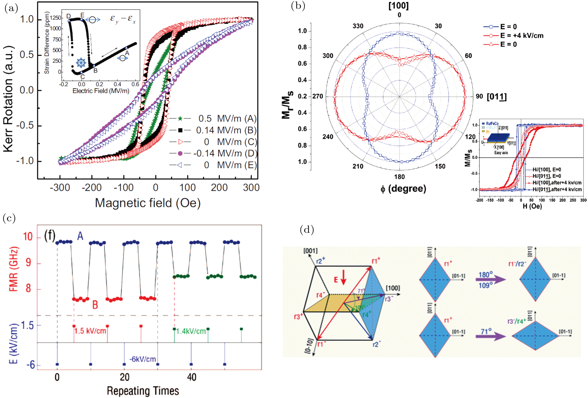 | Fig. 3. (color online) (a) Normalized Kerr rotation hysteresis curves along the  |
In 2012, Zhang et al. first reported on loop-like and non-volatile magnetization manipulation in amorphous CoFeB/(001) PMN-PT by a bipolar poling E-field.[54] Figure
 | Fig. 4. (color online) (a) Repeatable high/low magnetization states (open circle) switched by pulsed E-fields (blue line) in CoFeB/(001)PMN-PT (from Fig. |
In order to determine the underlying mechanism of the distinct modification behaviors, Yang et al. studied the strain response of the special type of (001) PMN-PT under continuous and pulsed E-field modes. This resulted in an asymmetric butterfly-like strain–electric (S–E) curve (Fig.
Epitaxial ferromagnetic film exhibits magnetocrystalline anisotropy, which originates from the spin–orbit coupling and correlates with the symmetry of the lattice structure. Compared to amorphous magnetic films with uniaxial magnetic anisotropy, iron-based epitaxial ferromagnetic films present biaxial magnetic anisotropy and the unique magnetization switching processes under magnetic fields.[57] Furthermore, FM films with cubic magnetocrystalline anisotropy (CMA) provide a pathway to realize multi-states magnetic information storage as long as one can precisely control the magnetization switching among the magnetocrystalline anisotropy determined energy minimum positions. Supposing a strain induced additional magnetic anisotropy is added to the film with CMA, the magnetic free energy without the external magnetic field is calculated. The simulated curves under different strain induced UMA clearly demonstrate that the magnetic easy axis rotates 90° from the initial direction (Fig.
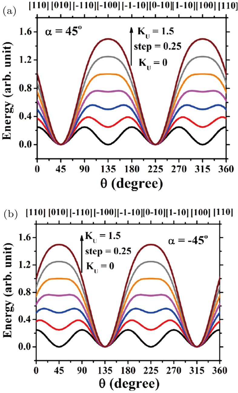 | Fig. 5. (color online) Theoretical calculations on the angular dependence of the free energy for strain-induced UMA energy along [010] (a) and [100] (b) directions (from Figs. |
Parkes et al. reported on a 90° non-volatile magnetization switching in epitaxial (001)FeGa/(001)GaAs/piezoelectric transducer heterostructures through transducer transferred strain when a voltage is applied.[59] In epitaxial (001)FeSi/(001)PMN-PT heterostructures with epitaxial relationships of FeSi(001)[100]//PMN-PT(001)[110], the magnetic anisotropy transition from four-fold CMA dominated to two-fold UMA dominated can occur subsequent to the application of negative E-fields in Fe86Si14/(001)PMN-0.32PT heterostructures. Unfortunately, the magnetic anisotropy transition is non-volatile and irreversible.[60] After modifying the composition of the ferromagnetic layer and the ferroelectric substrate, the angular dependence of the remanence (ARM) curves changes rapidly from the original four-fold to two-fold symmetries under E-fields in epitaxial Fe80Si20/(001)PMN-0.3PT. Moreover, the non-volatile and reversible 90° magnetization switching with the dominated UMA under ± 6 kV/cm is also observed. By measuring the micro-areas with a focused magneto-optical Kerr magnetometer under an E-field, the internal competitive relationship between the CMA energy and the UMA energy is confirmed by changing the shape of the M–H loop, as shown in Figs.
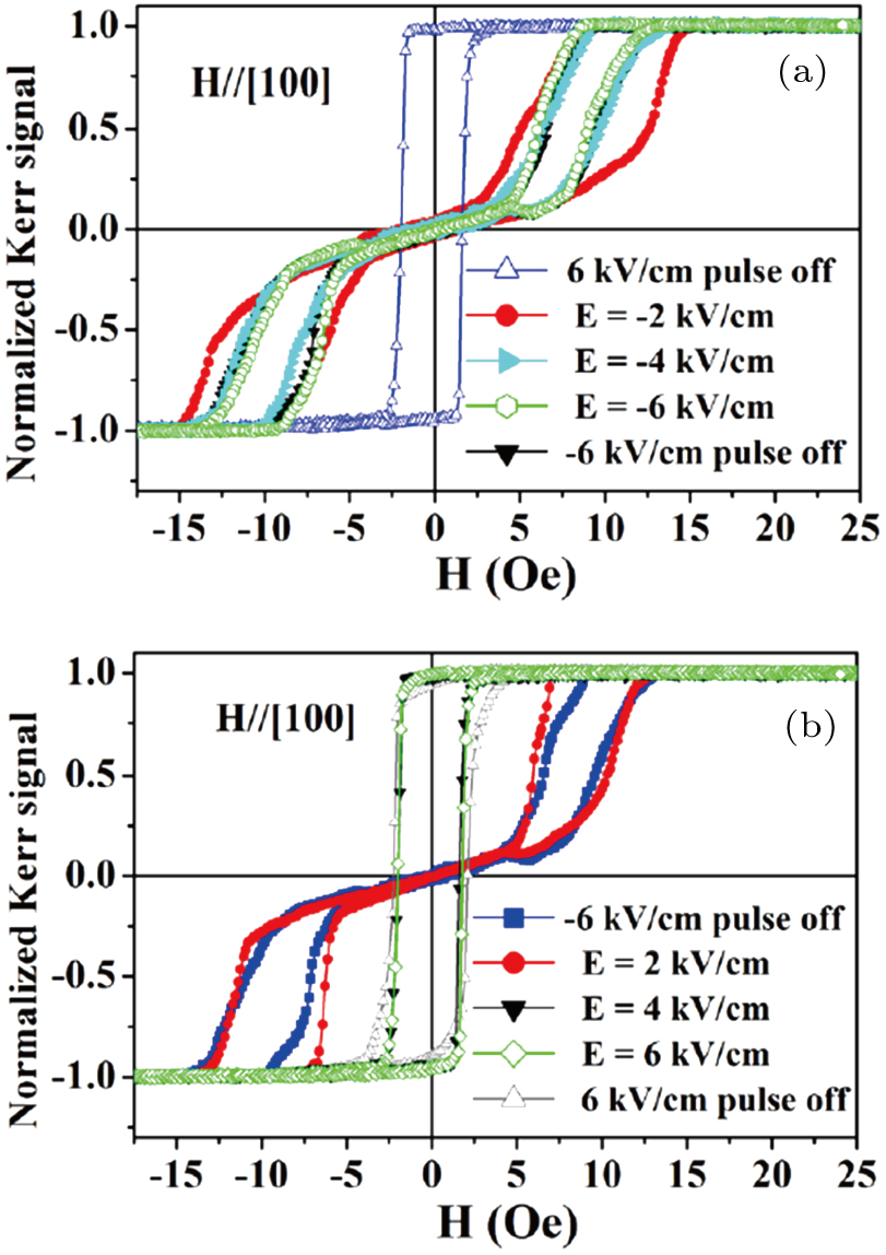 | Fig. 6. (color online) Normalized Kerr M–H loops along [100] direction under negative (a) and positive (b) E-fields in Fe80Si20/(001)PMN-0.3PT (from Figs. |
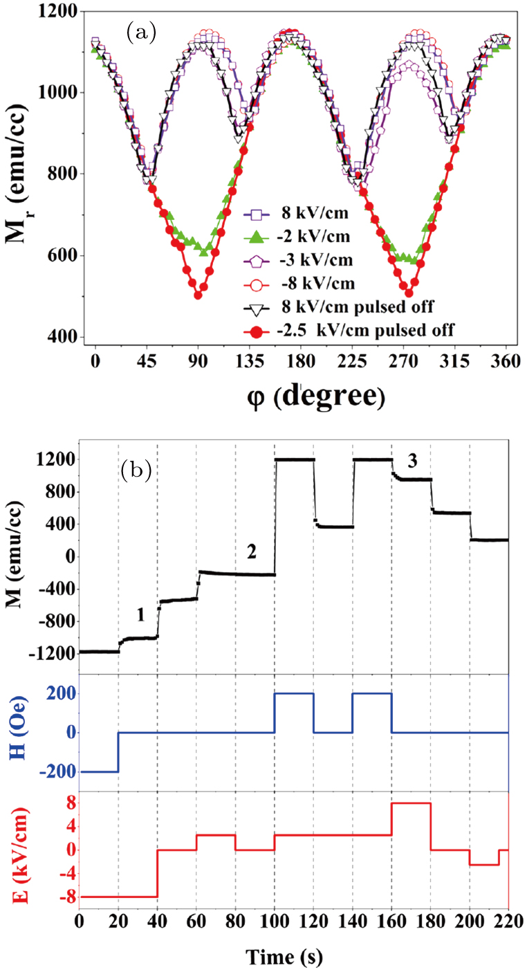
In Fe86Si14/(001)PMN-0.32PT and Fe80Si20/(001)PMN-0.3PT heterostructures, a feasible method for recovering the original CMA state is to anneal the heterostructures at a temperature of 150 °C.[58,60] However, in the epitaxial Fe80Si20/(011)PMN-0.3PT heterostructure at 300 °C post annealing, the release of interface strain leads to the reorientation of the dominated CMA when the E-field changes from −2.5 kV/cm to 8 kV/cm or from 2.5 kV/cm to −8 kV/cm. Conversely, when the E-field changes from 8 kV/cm to −2.5 kV/cm or from −8 kV/cm to 2.5 kV/cm, the two-fold dominated UMA changes back to four-fold CMA. Both kinds of magnetic anisotropies transitions are non-volatile and reversible (Fig.
In MTJs, the parallel/anti-parallel magnetization of two ferromagnetic electrodes gives rise to distinguishable low/high resistance states. However, manipulating full 180° magnetization reversal of the free layer without external magnetic fields is a challenge in MRAM design with the low-power requirements. Given the rapid development of E-field control 90° magnetization reversal, intense attention has been directed at E-field controlled 180° magnetization switching in FM films with the in-plane or perpendicular magnetic anisotropy.
In addition to the expected non-volatile 90° rotation of EA under E-fields, non-volatile in-plane 180° magnetization reversal in Co/(001) PMN-PT with the aid of a small auxiliary magnetic field was also achieved at room temperature. As shown in Fig.
 | Fig. 8. (color online) (a) Pulsed electrical operation with Hau (top) and the resulting magnetization (bottom) measured in a magnetic field of 3 Oe along [010] (from Figs. |
Compared with FM films with in-plane magnetic anisotropy, FM films with perpendicular magnetic anisotropy (PMA) have useful applications in STT-MARMs and SOT-MRAMs because they can effectively enhance the storage density.[68,69] It is accepted that PMA mainly originates from the interfacial magnetic anisotropy in ultrathin films, and the in-plane magnetic anisotropy results from the bulk magnetic anisotropy including the magnetocrystalline, random anisotropy or shape anisotropy. Therefore, the spin reorientation transition (SRT) is usually modified by changing the thickness of the films.[70–72] In (Co/Pt)3/(011)PMN-PT heterostructures, both the interface and the bulk contributions to anisotropy coexist at a critical Co layer thickness range. Sun et al. first reported on E-field manipulation of the interface magnetic anisotropy and SRT of (Co/Pt)3 multilayer at the critical thickness.[73] E-field modified variation of the first order volume anisotropy and interface anisotropy are 0.88% and −5.2%, respectively, whereas the E-field effect on the second-order volume anisotropy and interface anisotropy is very weak (Fig.
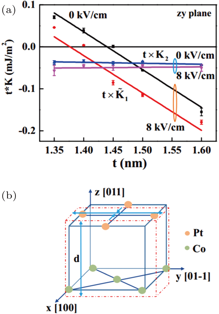 | Fig. 9. (color online) (a) Plots of   |
Recently, heavy metal/FM (HM/FM) bilayers with PMA received significant attention because they can utilize current induced SOT to realize magnetization switching.[12,75] Due to the strong SOC effect in HMs, their in-plane charge current can be converted to a pure spin current or interfacial spin accumulation by the spin Hall effect or Rashba effect, from the inversion asymmetry interface. The spin diffuses into the adjacent FM layer and switches the magnetization orientation through the SOT effect. In this process, a small in-plane assisted magnetic field is necessary to realize the 180° perpendicular magnetization reversal.[11,76] This is not convenient for practical applications. Thus, many investigations are focused on the realization of deterministic magnetization switching without any magnetic fields.[77–79] Cai et al. demonstrated deterministic magnetization switching in the symmetric Pt/Co/Ni/Co/Pt/(001) PMN-PT heterostructure combined with the E-field effect and the current effect.[80] As shown in the measurement schematic of Fig.
 | Fig. 10. (color online) (a) Schematic diagram of the measurement set-up. The voltage is applied to the PMN-PT substrates along the x-direction with a distance of 1 mm between the two electrodes. The applied voltage of VPMN-PT was removed during the current switching measurements. (b), (c) The current-induced magnetization switching after the polarization with the voltages of +500 V and −500 V on the PMN-PT substrate. (d) The deterministic magnetization switching by a series of current pulses applied to the device with 3-nm-thick bottom Pt layer. A small current IM (∼ 0.1 mA) was applied to measure the Hall resistance to distinguish the magnetization state (from Fig. |
In this review, we provided a summary of E-field controlled magnetization switching and magnetic anisotropy transition with an emphasis on the strain-mediated magnetism in FM/FE heterostructures. By considering volatile to non-volatile magnetization switching, isotropic to UMA to CMA variations, and in-plane UMA to out-of-plane PMA materials, we discussed the developments of E-field controlled macro scale magnetism variation based on special experimental or theoretical results for electric field generated strain in FM/FE heterostructures. However, some outstanding issues still need to be solved, which range from understanding the fundamental physical mechanism of an operation to the realization of practical applications.
(I) Since materials like PMN-PT used by many research groups are nominally the same, the observed E-field controlled converse ME responses were multifarious. Hence, more attention should be paid to the repeatability and the stability of the experimental results, as well as the intrinsic physical mechanism of the electric field induced magnetization switching.
(II) E-field controlled magnetization switching paves the way to a new generation of spintronic devices. However, the existing difficulties need to be addressed with regards to integration and miniaturization for magnetic storage applications, such as MRAM combined with the GMR or TMR effect.
| [1] | |
| [2] | |
| [3] | |
| [4] | |
| [5] | |
| [6] | |
| [7] | |
| [8] | |
| [9] | |
| [10] | |
| [11] | |
| [12] | |
| [13] | |
| [14] | |
| [15] | |
| [16] | |
| [17] | |
| [18] | |
| [19] | |
| [20] | |
| [21] | |
| [22] | |
| [23] | |
| [24] | |
| [25] | |
| [26] | |
| [27] | |
| [28] | |
| [29] | |
| [30] | |
| [31] | |
| [32] | |
| [33] | |
| [34] | |
| [35] | |
| [36] | |
| [37] | |
| [38] | |
| [39] | |
| [40] | |
| [41] | |
| [42] | |
| [43] | |
| [44] | |
| [45] | |
| [46] | |
| [47] | |
| [48] | |
| [49] | |
| [50] | |
| [51] | |
| [52] | |
| [53] | |
| [54] | |
| [55] | |
| [56] | |
| [57] | |
| [58] | |
| [59] | |
| [60] | |
| [61] | |
| [62] | |
| [63] | |
| [64] | |
| [65] | |
| [66] | |
| [67] | |
| [68] | |
| [69] | |
| [70] | |
| [71] | |
| [72] | |
| [73] | |
| [74] | |
| [75] | |
| [76] | |
| [77] | |
| [78] | |
| [79] | |
| [80] |


