Influence of dopant concentration on electrical quantum transport behaviors in junctionless nanowire transistors
Ma Liu-Hong1, 3, Han Wei-Hua2, 3, †, Zhao Xiao-Song2, 3, Guo Yang-Yan2, 3, Dou Ya-Mei2, 3, Yang Fu-Hua3, 4, ‡
School of Physical Engineering, Zhengzhou University, Zhengzhou 450001, China
School of Electronic, Electrical and Communication Engineering, University of Chinese Academy of Sciences, Beijing 100049, China
Engineering Research Center for Semiconductor Integrated Technology, Beijing Engineering Center of Semiconductor Micro-Nano Integrated Technology, Institute of Semiconductors, Chinese Academy of Sciences, Beijing 100083, China
State Key Laboratory for Superlattices and Microstructures, Institute of Semiconductors, Chinese Academy of Sciences, Beijing 100083, China


† Corresponding author. E-mail: weihua@semi.ac.cn fhyang@semi.ac.cn

Project supported by the National Key Research and Development Program of China (Grant No. 2016YFA0200503), the Program for Innovative Research Team (in Science and Technology) in University of Henan Province, China (Grant No. 18IRTSTHN016), and the National Natural Science Foundation of China (Grant Nos. 61376096, 61327813, and 61404126).

Abstract

We discuss the random dopant effects in long channel junctionless transistor associated with quantum confinement effects. The electrical measurement reveals the threshold voltage variability induced by the random dopant fluctuation. Quantum transport features in Hubbard systems are observed in heavily phosphorus-doped channel. We investigate the single electron transfer via donor-induced quantum dots in junctionless nanowire transistors with heavily phosphorus-doped channel, due to the formation of impurity Hubbard bands. While in the lightly doped devices, one-dimensional quantum transport is only observed at low temperature. In this sense, phonon-assisted resonant-tunneling is suppressed due to misaligned levels formed in a few isolated quantum dots at cryogenic temperature. We observe the Anderson-Mott transition from isolate electron state to impurity bands as the doping concentration is increased.

1. Introduction

In recent years, due to the advanced micro/nano-fabrication technologies,[1,2] the typical channel length of metal–oxide–semiconductor field-effect transistors (MOSFETs) has dropped to 10 nm. The rapid downscaling of MOSFETs has made the number of impurities sharply reduced in the channel. In nanoscale channel, the random distribution of dopants greatly influences the conductivity of devices.[35] In the case of nanowire device, a single impurity can easily affect the entire carrier flow. The effects of single dopants in the channel of a silicon device have been characterized in recent years.[6] The carrier behavior will be dominated by quantum mechanism and tunneling at low temperatures. Single electron transport mediated by individual dopants in silicon transistors has been observed, in particular at low temperatures below 20 K.[79] Previous publications which describe the influence of local donor induced quantum dots (QDs) on electrical characteristics mostly focus on inversion-mode transistors. The junctionless nanowire transistor (JNT), considered as a gated resistance with uniform doping, has been recently proposed as a promising alternative for a new generation of transistors.[10] Compared to the inversion-mode transistors, carrier in the JNTs flows in the middle of the channel rather than in the thin surface inversion layer. Hence, JNT leads to a more apparent quantum-confinement effect on the carrier transport and can provide a unique opportunity to probe the dopant fluctuation effects on the carrier transport in low dimensions.[11,12] At the initial stage of subthreshold, the lowest potential is formed in the electrical center. The potential landscape of the conduction path is modified by the dopant number. Consequently, the doping concentrations will significantly influence the carrier transport characteristics.

2. Device fabrication

To ensure high current drive as well as full depletion of all the channel region, the suitable doping density of the fabricated junctionless transistor is 2 × 1018 cm−3 ∼ 1 × 1019 cm−3.[10] In this paper, heavily-doped and lighter-doped JNTs with the channel length of 280 nm are fabricated. We investigate the influence of dopant concentration on the quantum transport patterns in long-channel JNTs. The features of quantum transport in Hubbard systems are only observed in heavily-doped device with a doping concentration of 1 × 1019 cm−3. While in the lighter-doped channel with a doping concentration of 2 × 1018 cm−3, no single electron transport is observed, and only one-dimensional quantum transport is observed. This work provides a basic qualitative description of electronic transport properties of random dopant fluctuation in nano-scale transistors.

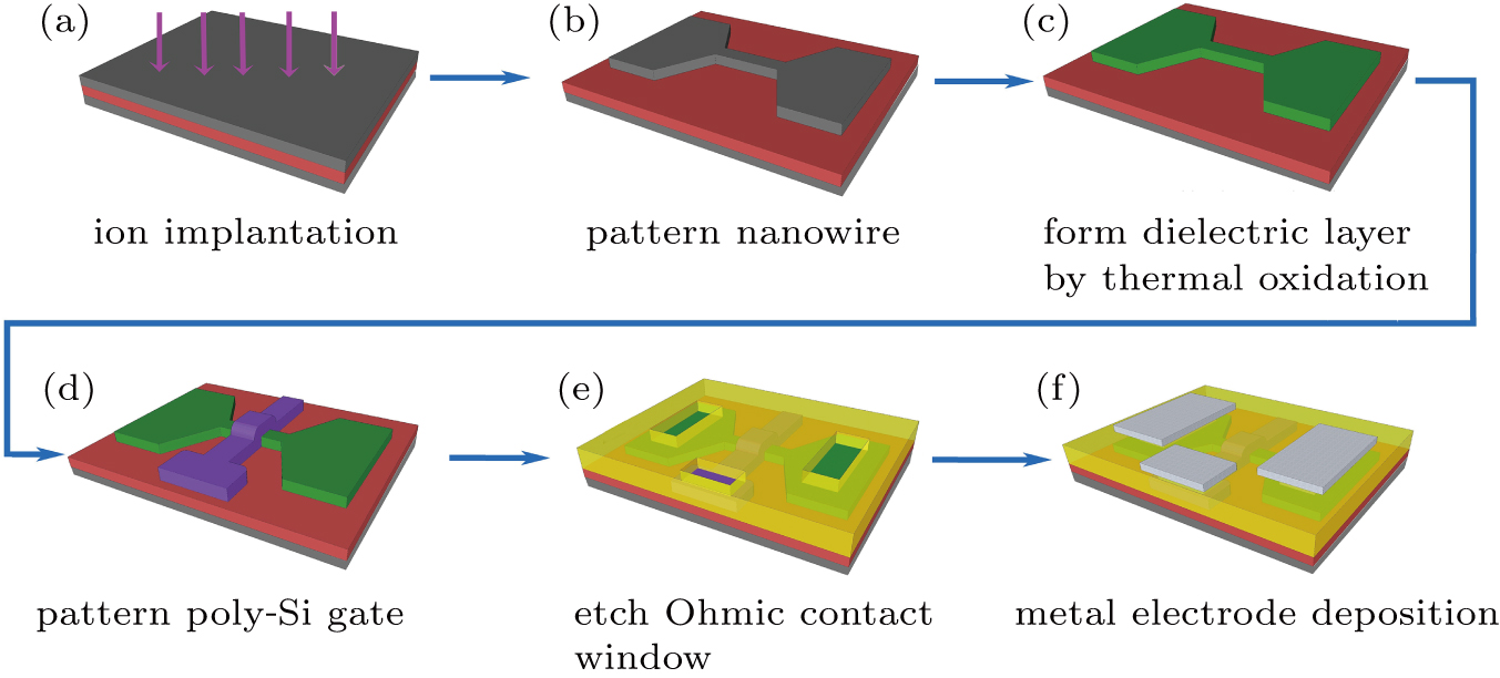
Figure 1 schematically shows the fabrication route of JNTs. Standard silicon on insulator (SOI) wafers were used as the substrate. After thermally growing 15 nm silicon dioxide as a buffer layer, the SOI wafer was uniformly doped by phosphorus ion implantation with a dose of 5 × 1013 cm−2 and 1 × 1013 cm−2, leading to a uniform concentration of 1 × 1019 cm−3 (type A) and 2 × 1018 cm−3 (type B), respectively. Next, the silicon fins were patterned with electron beam lithography (EBL) and inductively coupled plasma (ICP) etch. Afterwards, the devices underwent a sacrificial oxidation step to smooth the surfaces of the silicon fins. And then a 22-nm thick gate oxide was grown in dry oxygen at 900 °C for 1 hour. The remaining silicon core had a height of 30 nm and a width ranging from 28 nm to 35 nm, and then a 280-nm poly-silicon gate was formed. The poly-silicon was doped by arsenic ion implantation at a dose of 1 × 1020 cm−3 and then annealed at 1000 °C for 10 seconds. The gate electrode pads were fabricated by the evaporation of 20-nm-thick Ti film to form an Ni/Si ohmic contact, and then 300-nm-thick Al film was used for final metallization via conventional optical lithography.

Fig. 1. (color online) Schematic diagrams of the fabrication process for JNTs. (a) The process began with n-type ion implantation in the top silicon layer. (b) Silicon fin and two connected pads were patterned by SEM and ICP etch. (c) A 22-nm thick SiO2 dielectric layer was grown by thermal oxidation process. (d) A heavily p-doped poly-silicon gate was etched by reactive ion etching. (e) Conventional photolithography and ICP etch with O2 plasma were employed to pattern the Ohmic contact windows. (f) The control gate electrodes were formed by a 200-nm thick aluminum layer.

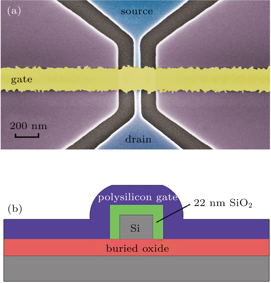
Figure 2(a) shows a scanning electron microscope (SEM) image of a fabricated JNT device. The fin has smooth and well-defined surface. Figure 2(b) shows the cross sectional view of the fabricated JNT with poly-silicon as the metal electrode, SiO2 as the gate dielectric, and (110)-oriented Si as the semiconducting channel material. Schematic diagram of the fabricated transistor structure has an extremely thin nanowire channel. The effect channel length is fixed to be 280 nm for all devices in this study to ensure the formation of multiple QDs.

Fig. 2. (color online) (a) False color SEM image and (b) cross sectional view of JNT.
3. Results and discussion

The fabricated JNTs were placed in a vacuum chamber which can be cooled down to 6 K with the help of Lakershore-340 temperature controller. As a whole, 100 samples have been studied electrically, mostly at a low temperature to observe the quantum effect in the narrow channel region. The doping concentrations of both types of devices show random dopant-induced threshold voltage fluctuations. Figure 3 shows the histograms of threshold voltage (Vth) distribution obtained from 8 JNTs with an average doping concentration of 1 × 1019 cm−3 at room temperature. We find a profound difference in the value of threshold voltage. It has been directly demonstrated that Vth fluctuation from 0 V to 0.6 V is caused by the statistical fluctuation of the dopant number in the channel layer.[13] That is, the absolute value of Vth increases with the increase of the dopant concentration, which has a larger effective doping concentration. While in the case of counter dopant number fluctuation, the absolute value of Vth becomes small. In junctionless transistor, dopant atoms are randomly located within the ultra-narrow channel at the initial stage of subthreshold. The random distribution of the dopants along the JNT channel plays a critical role in determining the barrier height and therefore the threshold voltage. Our measurement results, which are observed in both types of doping concentrations, well indicate that the dopant-induced fluctuation can be observed in dopant-rich environment, due to remarkable quantum confinement in JNTs.
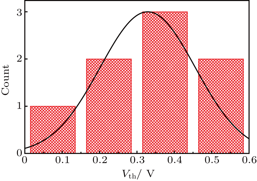
Fig. 3. (color online) Distribution of threshold voltages calculated for devices with a doping concentration of 1 × 1019 cm−3. All measured devices have a cross section of 35 nm × 30 nm.

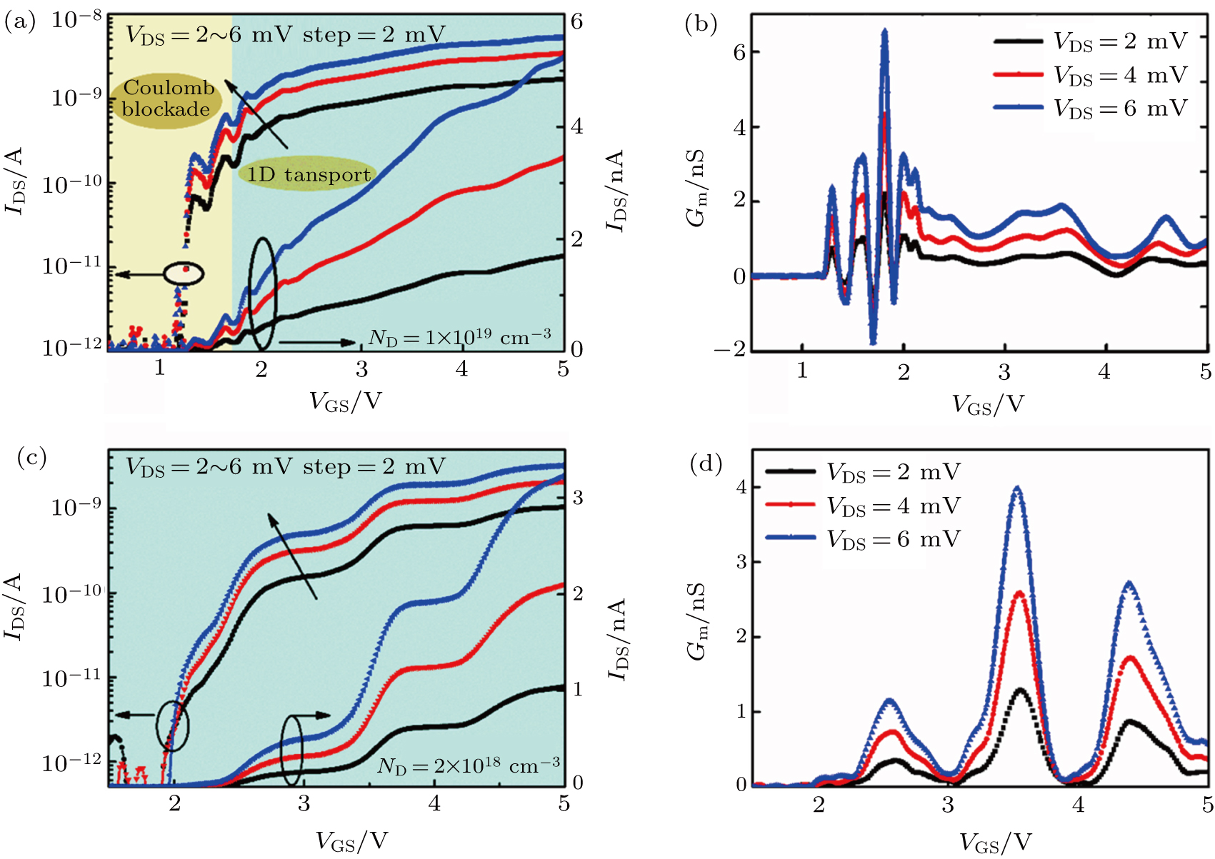
Figure 4(a) shows the drain current IDS as a function of the gate voltage VGS measured at 6 K for the device with a doping concentration 1 × 1019 cm−3. At initial stage of the transfer characteristics, remarkable current envelopes are clearly observed, which is due to the presence of multiple QDs in the narrow channel.[14] A one-dimensional (1D) QD array induced by multiple ionized donors is formed in the 280-nm length channel, providing an ultranarrow conduction path at low VGS. Larger current plateaus are observed above the flatband voltage, which is characteristic for 1D quantum transport. In general, the electron transport system is evolving from coulomb blockade regime to 1D regime with increased VGS. The transconductance trance (GmVGS) shown in Fig. 4(b) can also provide a better understanding of the evolution process of carrier transport mechanisms. The typical IDSVGS characteristic and GmVGS characteristic curves measured at low temperature of 6 K for type-B device are presented in Figs. 4(c) and 4(d), respectively, for different values of source-drain (VDS) bias ranging from 2 mV to 6 mV in increments of 2 mV. A noteworthy feature is the deficiency of coulomb current oscillations near subthreshold voltage, and only 1D quantum transport characterized by current plateaus is observed. In other words, no effective conduction path is formed by ionized donors induced QDs for the lighter doping JNTs at the initial stage of subthreshold.

Fig. 4. (color online) (a) IDSVGS and (b) GmVGS characteristics of a typical type-A device measured at 6 K. The applied VDS range from 2 mV to 6 mV in increments of 2 mV. (b) IDSVGS and (d) GmVGS characteristics of a typical type-B device measured at 6 K.

Through the above analysis, we can make sure that the electron transport mechanism through QDs is totally different at the initial stage of subthreshold. To obtain the root cause of the difference in transport mechanism, fundamental studies about the behavior of individual ionized donor in the channel should be performed. We obtained the density of ionized impurity atoms in the channel by the expression[15] where b = 1/[1 + (ND/Nb)d], n1 = NC exp(−ED/kBT), and ED is the donor ionization energy. Here NC is the effective density of states in conduction band, given by , with being the effective mass of electron, and MC = 6 corresponding to the number of conduction band minima. For phosphorus-doped silicon, the values of the parameters g, d, and Nb are 1/2, 2.3, and 6 × 1018 cm−3, respectively. It should be noted that n is the free electron density which is generated from ionized impurities by the intrinsic excitation and the thermal activation. At such low temperature of 6 K, the number of free electrons generated by the intrinsic excitation is negligible. Hence, the ionized rate in Eq. (1) can be safely approximated under the condition of . According to the model proposed by Altermatt et al., the ionization energy ED depending on the doping concentration ND is described by[16] For phosphorus-doped crystalline silicon, ED0 = 45.5 meV, Nref = 2.2 × 1018 cm−3, and c = 2. When ND = 1 × 1019 cm−3 and 2 × 1018 cm−3, ED is equal to 2.1 meV and 24.9 meV, respectively. As the doping concentration increases, the ionized energy decreases, especially for heavily doping semiconductor. The ionization rate calculated using the Alternate model is presented in Fig. 5 as a function of temperature. It is clear that the ionization is very close to unity as the doping concentration increases. Hence, we estimate that the doping efficiency at 6 K is about 78% for type-A device and 25% for type B device.

Fig. 5. (color online) Ionization ratio as a function of temperature for several doping concentrations.

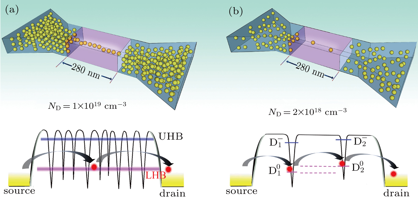
At high doping concentrations of ND = 1 × 1019 cm−3 (above the metal-insulator transition concentration), most donors are ionized even at low temperature. If we assume the size of the initial conduction path is comparative to the Bohr radius of 2 nm for phosphorus atom in silicon, the average number of ionized donors in the conductive path of type-A JNT is approximately 9 (2 nm × 2 × 280 nm × 1 × 1019 cm−3 × 78%). Considering the statistical variation, the ionized donor number may vary from 6 to 12.[13] The coupled QDs array can be formed by a number of phosphorus donors positioned closely to each other, due to the strong interaction between neighboring ionized donors. Therefore, in the system of multiple coupled ionized donors, the neutral state D0 and the negatively charged state D state develop into two impurity bands, i.e., the lower Hubbard band (LHB) and upper Hubbard band (UHB).[17] For this type of device, as schematically illustrated in Fig. 6(a), conductance occurs dominantly by resonant tunneling via Hubbard bands, which manifests as coulomb blockade. As a consequence, two large current envelops are observed below the threshold voltage. The conductance of the two Hubbard bands is in good agreement with Mott theory as applied to doped semiconductor. The measured resonant tunneling characteristics are the hallmark to identify Hubbard impurity bands generated by unintentionally deterministic doping QDs.

Fig. 6. (color online) Nanoscale JNTs under the subthreshold conduction with different channel-doping profiles. (a) Illustrations of possible dopant arrangements and expected potentials landscapes induced by a larger number of ionized donors forming multiple-coupled QDs for type-A devices. (b) A possible potential landscape induced by a few isolated, ionized donors for type-B devices.

We now turn to the behaviors of QDs formed in the JNT channel with the doping density of 2 × 1018 cm3. In case B, the average number of ionized donors in the conductive path below the gate is one. Consequently, none or only a small number of QDs are formed in the center of the channel below the threshold. When elastic tunnel process is the dominant transport mechanism, electron through a few QDs is resonantly enhanced only when the levels of QDs are aligned. Actually, localized quantum states of QD are different from each other with regard to the random distribution of donors. Resonant tunneling through double QDs is illustrated in Fig. 6(b). In nonresonant inelastic tunneling, an electron can hop through the QDs nonresonantly by absorbing the activation energy.[18] The diagram of the electron energies in the dot indicates that an electron needs to absorb the activation energy in order to contribute to the current. Otherwise, electron will be “trapped” within QDs. The trapped electron in the QD has a small range of energy variation taking into account the thermal energy EC ≈ 0.52 meV at low temperature of 6 K. Misaligned dot to dot transport via nearest-neighbor hopping rate is lowed. According to Mott’s theory for disordered QDs system at low temperature, the electron can hop a mean distance larger than the nearest-neighbor separation to find a further QD but with closer energy.[19] This variable-range-hopping transport mechanism will involve three or more QDs. However, the chance of multihop conduction is slim, due to the lack of sufficient QDs. Then electron hop occurs neither directly via nearest-neighbor hopping nor variable-range hopping in long channel with a few QDs out of alignment. In this case, electron tunneling through QDs in the channel of type-B devices is totally suppressed. For effective conduction path to be formed, the gate voltage should be increased more positively to ensure broadened neutral region in the channel. Above the threshold voltage, the dopant-induced potential fluctuation is screened by trapped electrons and the barrier is lowed by higher gate voltage, and 1D conduction path would then be formed. We can observe 1D quantum transport above the threshold voltage in both two types of devices at the higher gate voltage.

4. Conclusion

In this work, we report the electrical measurement results of two types of n-doped JNTs with different doping concentrations at low temperature. The influence of doping concentration on the electrical characteristics of JNTs is investigated. Donor-induced fluctuation is observed even in heavily doped device, resulting in threshold voltage fluctuation. The electron transport behavior is significantly different depending on whether phosphorus donors in the channel region are strongly coupled with each other. Strongly-coupled dopants control the Hubbard bands conductance in nanoscale transistors with heavily doping concentration of 1 × 1019 cm−3. While in JNT channel with a lighter doping concentration of 2 × 1018 cm−3, conduction path belongs to the isolated donor regime and forms misaligned localized quantum states. The transport mechanisms extracted from the electrical measurements provide important information on quantum states of donors in subthreshold regime.

Reference
[1] Wagner C Harned N 2010 Nat. Photon. 4 24
[2] Wang W Su Y F Liu C R Li D X Wang P Duan Z Y 2015 Chin. Phys. Lett. 32 128102
[3] Nayak K Agarwal S Bajaj M Murali K V Rao V R 2015 IEEE Trans. Electron Dev. 62 685
[4] Akhavan N D Ferain I Yu R Razavi P Colinge J P 2012 Solid-State Electron. 70 92
[5] Li Y Hwang C H 2007 J. Appl. Phys. 102 084509
[6] Tabe M Moraru D Ligowski M Anwar M Jablonski R Ono Y Mizuno T 2010 Phys. Rev. Lett. 105 016803
[7] Fuechsle M Miwa J A Mahapatra S Ryu H Lee S Warschkow O Simmons M Y 2012 Nat. Nanotechnol. 7 242
[8] Moraru D Samanta A Anh L T Mizuno T Mizuta H Tabe M 2015 Sci. Rep. 4 6219
[9] Pierre M Wacquez R Jehl X Sanquer M Vinet M Cueto O 2010 Nat. Nanotechnol. 5 133
[10] Colinge J P Lee C W Afzalian A Akhavan N D Yan R Ferain I Razavi P O–Neill B Blake A White M 2010 Nat. Nanotechnol. 5 225
[11] Ma L H Han W H Wang H Lyu Q F Zhang W Yang X Yang F H 2016 Chin. Phys. 25 068103
[12] Park J T Kim J Y Lee C W Colinge J P 2010 Appl. Phys. Lett. 97 172101
[13] Mizuno T Okumtura J Toriumi A 1994 IEEE Trans. Electron. Dev. 41 2216
[14] Prati E Hori M Guagliardo F Ferrari G Shinada T 2012 Nat. Nanotechnol. 7 443
[15] Altermatt P P Schenk A Heiser G 2006 J. Appl. Phys. 100 113715
[16] Altermatt P P Schenk A Heiser G 2006 J. Appl. Phys. 100 113714
[17] Mott N F Davis E A 2012 Electronic Processes in Non-Crystalline Materials Oxford Clarendon Press
[18] Ma L H Han W H Wang H Hong W T Lyu Q F Yang X Yang F H 2015 J. Appl. Phys. 117 034505
[19] Rosenbaum R 1991 Phys. Rev. 44 3599