Project supported by the National Key Research and Development Program of China (Grant Nos. 2018YFA0305700 and 2016YFA0401804), the National Natural Science Foundation of China (Grant Nos. 11574323, 11704387, U1632275, 11304321, 11604340, and 61774136), the Natural Science Foundation of Anhui Province, China (Grant No. 1708085QA19), and the Director’s Fund of Hefei Institutes of Physical Science, Chinese Academy of Sciences (Grant No. YZJJ201621).
Project supported by the National Key Research and Development Program of China (Grant Nos. 2018YFA0305700 and 2016YFA0401804), the National Natural Science Foundation of China (Grant Nos. 11574323, 11704387, U1632275, 11304321, 11604340, and 61774136), the Natural Science Foundation of Anhui Province, China (Grant No. 1708085QA19), and the Director’s Fund of Hefei Institutes of Physical Science, Chinese Academy of Sciences (Grant No. YZJJ201621).
† Corresponding author. E-mail:
Project supported by the National Key Research and Development Program of China (Grant Nos. 2018YFA0305700 and 2016YFA0401804), the National Natural Science Foundation of China (Grant Nos. 11574323, 11704387, U1632275, 11304321, 11604340, and 61774136), the Natural Science Foundation of Anhui Province, China (Grant No. 1708085QA19), and the Director’s Fund of Hefei Institutes of Physical Science, Chinese Academy of Sciences (Grant No. YZJJ201621).
PtS2, which is one of the group-10 transition metal dichalcogenides, attracts increasing attention due to its extraordinary properties under external modulations as predicted by theory, such as tunable bandgap and indirect-to-direct gap transition under strain; however, these properties have not been verified experimentally. Here we report the first experimental exploration of its optoelectronic properties under external pressure. We find that the photocurrent is weakly pressure-dependent below 3 GPa but increases significantly in the pressure range of 3 GPa–4 GPa, with a maximum ∼ 6 times higher than that at ambient pressure. X-ray diffraction data shows that no structural phase transition can be observed up to 26.8 GPa, which indicates a stable lattice structure of PtS2 under high pressure. This is further supported by our Raman measurements with an observation of linear blue-shifts of the two Raman-active modes to 6.4 GPa. The pressure-enhanced photocurrent is related to the indirect-to-direct/quasi-direct bandgap transition under pressure, resembling the gap behavior under compression strain as predicted theoretically.
Transition metal dichalcogenides (TMDs), as a typical class of two-dimensional (2D) materials similar to graphene and black phosphorus, have attracted much attention because of their physical properties and promising potential applications in the field of electronics and optoelectronics.[1–7] Due to the quasi-2D nature of their lattice, they possess unique electronic band structure that can be effectively tuned by methods such as layer-dependence controlling, intercalating a variety of organic molecules, alkali or transition metals between the layered structures, applying pressure, mechanical strain or external electric fields on these materials.[6,8–18] For example, Mak et al. showed that decreasing the thickness of MoS2 induces a crossover of the bandgap from indirect one in bulk material to a direct-gap in monolayer, which causes a strong enhancement of light emission as well as an increase of luminescence quantum efficiency by more than 4 orders of magnitude.[8] In addition, the intercalation of C3H5NH2 molecules between layers of NbSe2 behaves as electron donors and increases interlayer separations, resulting in profound changes in the electronic structure of the host lattice to induce an obvious increase of optical absorption.[11]
A computational study revealed that the electron mobilities of PtS2 can be as high as ∼ 4000 cm2/V·s, which is among the highest in the selected TMDs.[4,5] Besides, PtS2 has a large tunable bandgap, ranging from 1.6 eV in monolayer, 1.2 eV in the bilayer, and ultimately to 0.25 eV in the bulk PtS2.[6] Recently, it was also shown that PtS2 exhibits excellent optoelectronic performance with high responsivity up to 1.56 × 10³ A/W and high detectivity of 2.9 × 10¹¹ Jones.[9] Density functional theory (DFT) calculations predicted that, when under a mechanical strain, the indirect bandgap of monolayer PtS2 becomes quasi-direct band-gap, which would be further in favor of the efficiency of light absorption and emission.[16]
In this paper, we employ high pressure means to manipulate the optoelectronic properties of PtS2. Experimentally, it has been shown that the high pressure indeed plays an effective role in tuning the electronic properties of TMDs.[19–21] We find that the photocurrent shows weak pressure dependence below 3 GPa but increases rapidly until a maximum at ∼ 4 GPa, of ∼ 6 times higher than that at ambient pressure. Further increase of pressure results in a metallization and hence a sharp drop of photocurrent at 5.6 GPa–6 GPa. X-ray diffraction patterns reveal that the lattice structure of PtS2 is ultra-stable under pressure, without observation of structural phase transition up to 26.8 GPa.
High-quality PtS2 single crystals were grown by chemical vapor transport method using phosphorus as transporting agent.[9] The mixture of Pt, S, and P powers in stoichiometric ratio 1:3:1 was placed inside an evacuated and sealed quartz tube. The tube was slowly heated up to 85 °C on one end while the other end was kept at 75 °C. After 20 days of growth, plate-like crystals were obtained on the cold end. High-pressure photocurrent and resistance were performed in a screw-pressure-type diamond anvil cell made of BeCu alloy which was measured in High Magnetic Field Laboratory of the Chinese Academy of Sciences. Diamond anvils of 300-μm culets and a T301 stainless-steel gasket covered with a mixture of epoxy and fine cubic boron nitride (c-BN) powder were used for high-pressure transport measurements. The two-probe method was applied in the ab plane of single crystals with typical dimensions of 70 μm × 40 μm × 10 μm. The high-pressure photocurrent was measured under the illumination of a 532-nm excitation laser with power of 8.5 mW. The in situ high-pressure synchrotron radiation x-ray diffraction (XRD) (λ = 0.3100 Å) experiments were carried out at 16-BM-D station of High-Pressure Collaborative Access at Advanced Photo Source of Argonne National Laboratory.[22] The DIOPTAS and RIETICA programs were employed for the image integrations and the XRD profile refinements, respectively.[23,24] The LeBail method was used to extract the lattice parameters. High-pressure Raman scattering experiments were carried out using a Raman spectrometer with a 532-nm excitation laser. The ruby fluorescence method was used to determine the pressure for all of the above experiments.[25]
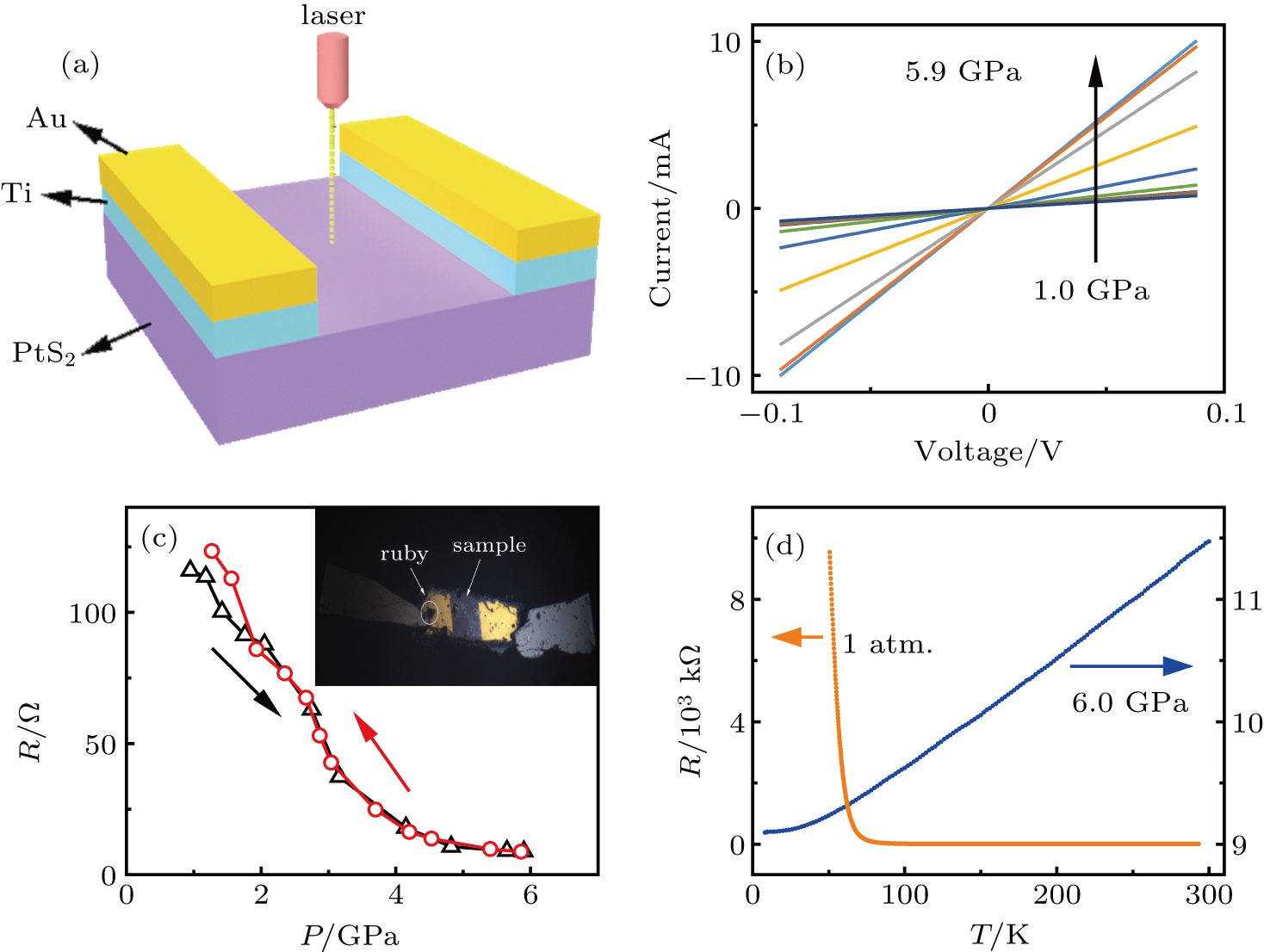
A PtS2-based device was fabricated for investigating the optoelectronic properties and transport properties under pressures. The sample configuration is illustrated in Fig.
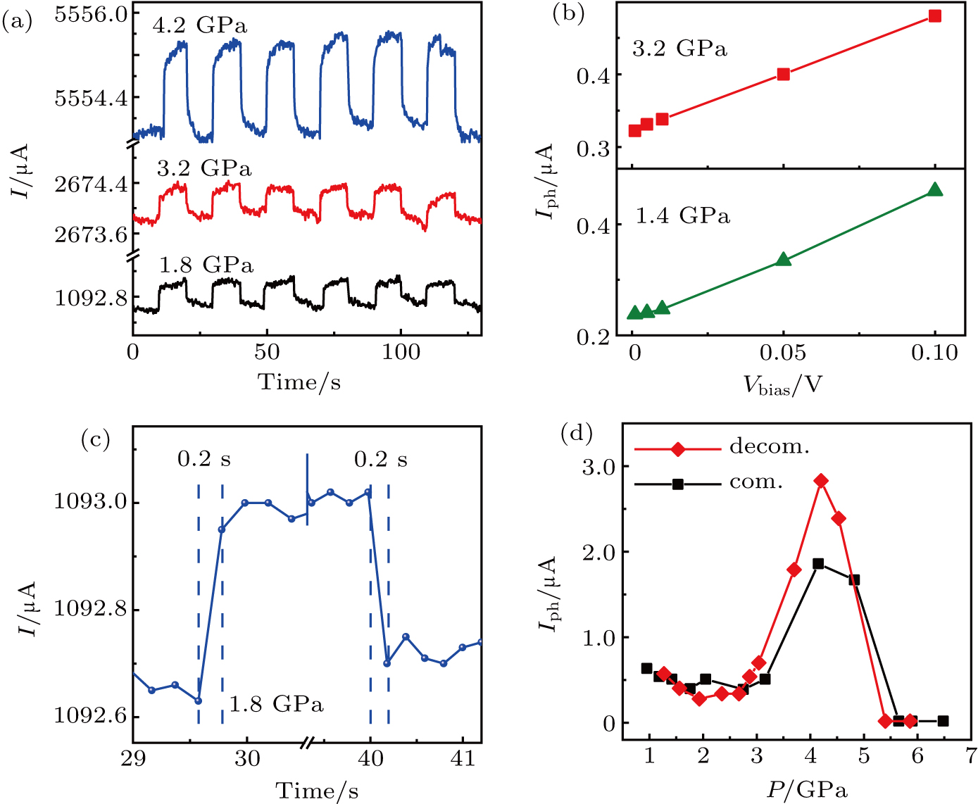
In order to examine the pressure effect on the optoelectronic properties of the PtS2 device, we measured the time-dependent current I–t under different applied pressures, by intentionally switching ON/OFF the incident light of 532-nm laser illumination. The current was measured under a bias voltage of 0.1 V, in a linear range of I(Vbias) (see Fig.
The values of photocurrent Iph = Iillumination – Idark under different pressures are extracted from the I–t pulses and then represented as a function of applied pressure in Fig.
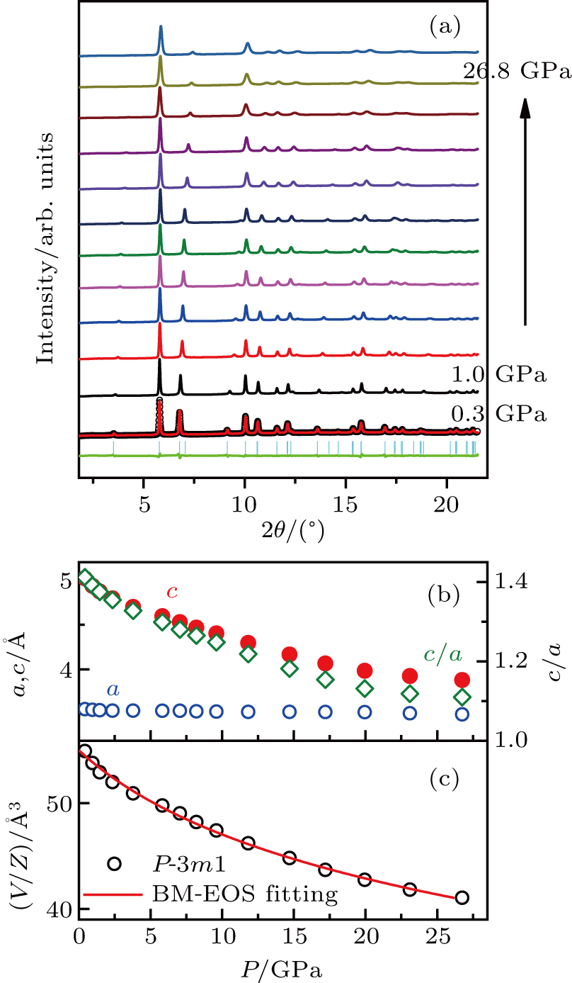
In some materials, such as ferroelectric photovoltaics KBiFe2O5, organic perovskite CH3NH3PbBr3 and CH3NH3SnI3, the variation of photoresponsivity (R = Iph/Peff, where Peff is the effective illumination power) is originated from pressure-driven structural phase transition as revealed by existing literatures.[26–28] Therefore, it is of great interest to clarify what is happening to the lattice structure during the compression for understanding the change of the optoelectronic properties and resistance under pressure. The high-pressure in situ synchrotron x-ray diffraction (XRD) study of the PtS2 sample was performed up to 26.8 GPa. Selected XRD spectra during compression procedures are displayed in Fig.
The detailed lattice parameters were obtained by refinement of the XRD patterns using the Lebail method. The starting fitting point of structural parameters of the hexagonal (P-3m1) phase were taken from the study of PtS2 by Furuseth et al., and the fitted parameters were used for the starting point of the next higher-pressure point.[29] As an example, the lines at the bottom of Fig.
 |
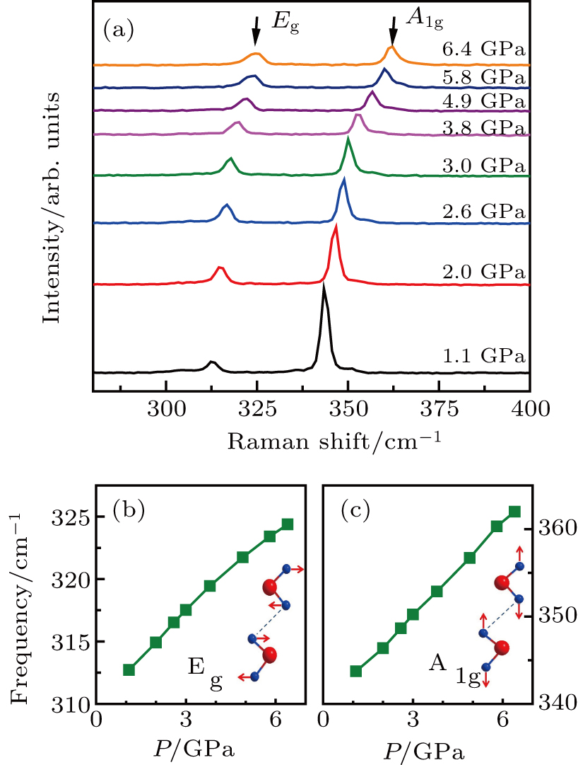
We further carried out a detailed Raman study on PtS2 under pressures up to 6.4 GPa, to further confirm that the sharp increase of photocurrent between 3 GPa–4 GPa is NOT due to a potential structural phase transition. Figure
With increasing pressure, the increase of relative intensity ratio of the Eg to A1g peaks may be attributed to the dominance of the in-plane lattice vibration when the lattice is more strongly compressed along the c direction. The evolutions of the frequencies of the two modes are displayed as functions of pressure in Figs.
Generally, the ability of a semiconductor to absorb light and to gain photogenerated carriers is directly influenced by the band structure.[31] For a semiconductor with a direct bandgap, photons with energy higher than the bandgap are readily to be absorbed, but for a system with indirect bandgaps, the efficiency of absorption of photons is much reduced due to the necessity of absorption of an additional phonon to supply the difference in momentum.[31] For example, benefiting from the direct nature of the bandgap in monolayer MoS2 in contrast to the indirect bandgap in bulk MoS2, the photoresponsivity (i.e., photocurrent per illumination power) of the monolayer MoS2 was significantly enhanced by ∼ 9000 times compared to that in multilayer devices.[32] For monolayer PtS2, as mentioned above, the density functional theory (DFT) calculations predict that a transition of the bandgap from an indirect nature to a quasi-direct one will take place when the system is under a mechanical strain,[16] which would be much in favor of the efficiency of light absorption and the yield of photogenerated carriers. Here in our PtS2 device, we show that under high pressure of 1 GPa–3 GPa the resistance firstly decreases monotonically without obvious change of the photocurrent observed, indicative of a continuous narrowing of the indirect bandgap. But then in the pressure range of 3 GPa–4 GPa, the photocurrent displays a sharp increase with a maximum enhancement of ∼ 6 times compared to that at ambient pressure. These facts can be attributed to a underlying transition of the bandgap under pressure from an indirect gap to a direct or quasi-direct gap. Further increase of the pressure results in a metallization of the system (as is proved by our temperature-dependent resistance measurements) and hence a sharp drop of the photocurrent down to almost zero. All these results fit together and establish that the high pressure is an effective method to tune the band structure of PtS2 and to improve the optoelectronic properties.
In summary, we report on the pressure-induced enhancement of optoelectronic properties in PtS2. It is found that the photocurrent is effectively improved by ∼ 600% at ∼ 4 GPa compared to that at ambient pressure, which is attributed to an underlying bandgap transition from an indirect one to a direct or quasi-direct one. Further increase of the applied pressure causes a metallization of the system at 5.6 GPa–6 GPa. High-pressure XRD results indicate no structural phase transition and an ultra-stability of the lattice under pressures up to 26.8 GPa. Our results reveal that pressure is a simple but effective tool to improve the optoelectronic properties of PtS2.
| [1] | |
| [2] | |
| [3] | |
| [4] | |
| [5] | |
| [6] | |
| [7] | |
| [8] | |
| [9] | |
| [10] | |
| [11] | |
| [12] | |
| [13] | |
| [14] | |
| [15] | |
| [16] | |
| [17] | |
| [18] | |
| [19] | |
| [20] | |
| [21] | |
| [22] | |
| [23] | |
| [24] | |
| [25] | |
| [26] | |
| [27] | |
| [28] | |
| [29] | |
| [30] | |
| [31] | |
| [32] |


