Pressure-induced enhancement of optoelectronic properties in PtS2
Project supported by the National Key Research and Development Program of China (Grant Nos. 2018YFA0305700 and 2016YFA0401804), the National Natural Science Foundation of China (Grant Nos. 11574323, 11704387, U1632275, 11304321, 11604340, and 61774136), the Natural Science Foundation of Anhui Province, China (Grant No. 1708085QA19), and the Director’s Fund of Hefei Institutes of Physical Science, Chinese Academy of Sciences (Grant No. YZJJ201621).
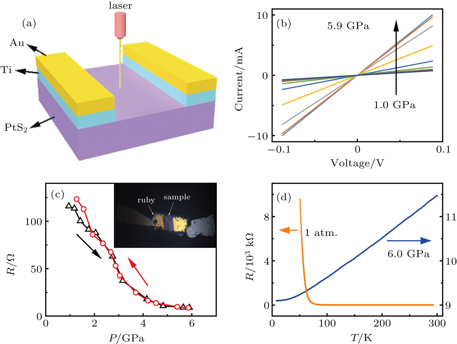
(a) Schematic illustration of the structure of fabricated PtS2 device. (b) The I–V curves of the PtS2 device measured at room temperature under different applied pressures. (c) Pressure dependence of the room-temperature resistance of the PtS2 device. Inset displays a microphotograph of the sample configuration in a DAC. (d) Temperature dependence of resistance measured under pressures of 1 atm (1 atm = 1.01325 × 10⁵ Pa). and 6 GPa.