1. IntroductionExchange bias (EB) is a physical phenomenon observed in a bilayer system comprised of FM/AFM (ferromagnetic/antiferromagnetic) systems. The origin of EB is mainly attributed to the pinning of spin in ferromagnetic layer by antiferromagnetic layer that leads to magnetic hysteresis loop shift and coercivity enhancement. The EB phenomenon is extensively applied to the fields of giant magnetoresistance (GMR) and tunneling magnetoresistance (TMR) by pinning the spin of the ferromagnetic layer used in them. The essence of EB is a kind of unidirectional anisotropy.[1] It was first discovered by Meiklejohn and Bean in the 1950s,[2] and the implication of that research has been lasting till now. The classical model[3] of EB was first proposed to explain the origin of bias field HB. However, the experimental HB was much smaller than the theoretical value. Mauri et al.,[4] Malozemoff,[5] and Koon[6] put forward their proposals to adjust the theoretical model. They pointed out that the difference originates mainly from the AFM spins that stabilize the pinning effect on the spins of the ferromagnetic layer. Besides the theoretical analysis, intensive experimental researches[7–11] have been carried out to investigate the underlying mechanism of FM/AFM exchange bias system which can present much useful information. Recently, the synchrotron radiation technology gave a new path to analyzing the AFM spin structure[7] through the measurements using X-ray magnetic linear dichroism (XMLD). Wu et al.[8] showed that in the epitaxial CoO/Fe/Ag (001) multilayer only ∼ 5% of frozen CoO spin was enough to establish EB, which means that the pinning effect was not homogeneous throughout the ferromagnetic layer. Also the visual investigation of asymmetry reversal processes in FM/AFM bilayer by magneto-optical indicator film (MOIF) technique,[9] magnetic force microscopy (MFM)[10] and magneto-optical Kerr effect (MOKE) microscopy[11] gave much useful information about the magnetic domain structure and the magnetization reversal mode. However, the direct observation of the AFM pinning effect is limited due to the low spatial resolution of the above magnetic imaging techniques.
Alternatively, Lorentz transmission electron microscopy (LTEM) is a powerful technique to acquire magnetic domain structure in high spatial resolution, which has already been widely used in the fields of permanent magnets,[12] soft magnetic materials,[13] magnetic nanowires[14] and magnetic skyrmions.[15] Previously some researches of EB by using LTEM were also carried out. For example, the differential phase contrast (DPC) technique in LTEM was used to observe the in-situ magnetization reversal process of the Co35Fe65(70 nm)/NiMn(50 nm) bilayer.[16] Also the observation of the 360° domain wall (DW), which was a very special magnetic domain structure, was found in the CoFeB/IrMn bilayer films by Kovás et al.[17] In this research, the dynamic domain structure of FM/AFM was observed, however, the pinning effect of AFM has not been analyzed nor discussed in detail.
In our work, we focus on the pinning effect of the AFM on FM to observe the magnetization reversal process of CoFeB/IrMn bilayer film. We select three samples, a single CoFeB layer, and two CoFeB/IrMn bilayer samples with weak and strong pinning effect to observe the difference between the dynamic behaviors of their magnetic domain reversals. We observe the complex magnetic reversal in strong pinning bilayer, which offers apparent experimental evidence to understand the nonuniform pinning effect from AFM layer.
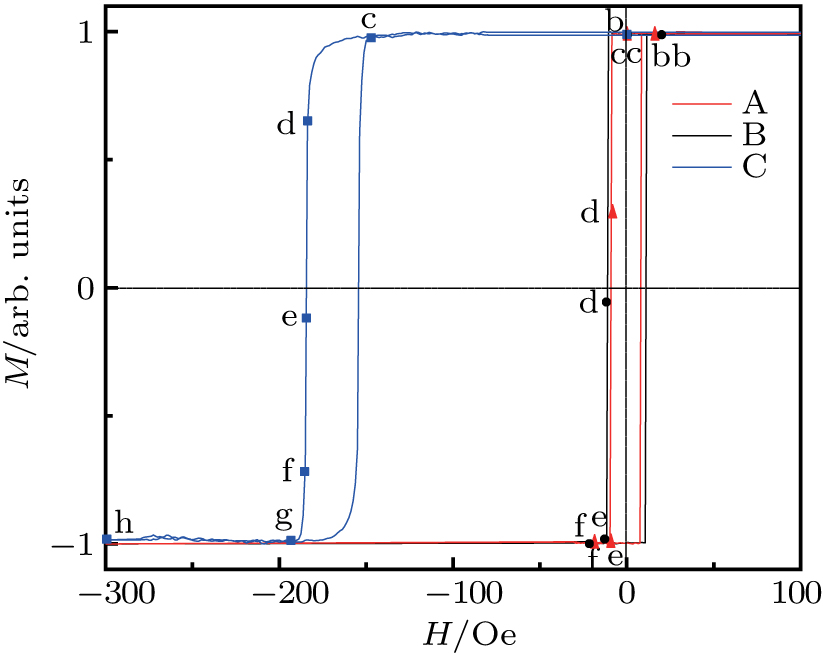
3. Results and discussionThree samples are comprised of CoFeB layers whose thickness values are fixed at 20 nm, and IrMn layers, whose thickness values are 0 nm, 5 nm, and 30 nm and correspond to sample A, sample B, and sample C, respectively. The magnetic characterizations of the samples are shown in Fig. 1. In this figure, sample A exhibits a standard soft magnetic nature with Hex 0 and coercivity 8 Oe. While sample B shows quite a small HEB, ∼ 1 Oe, and a little larger coercivity of 11 Oe with the increase of the IrMn layer thickness tIrMn. Further increase of tIrMn to 30 nm (sample C) leads to the increase of HEB to 170 Oe, and the coercivity also increases a little (to 15 Oe). From the loops, it is shown that the squareness of sample A and that of sample B are both larger than that of sample C. It is considered that the AFM/FM pinning effect increases from sample B to sample C, and the dynamical magnetization reversals at the descending branches in hysteresis loops of all three samples are observed for comparison.
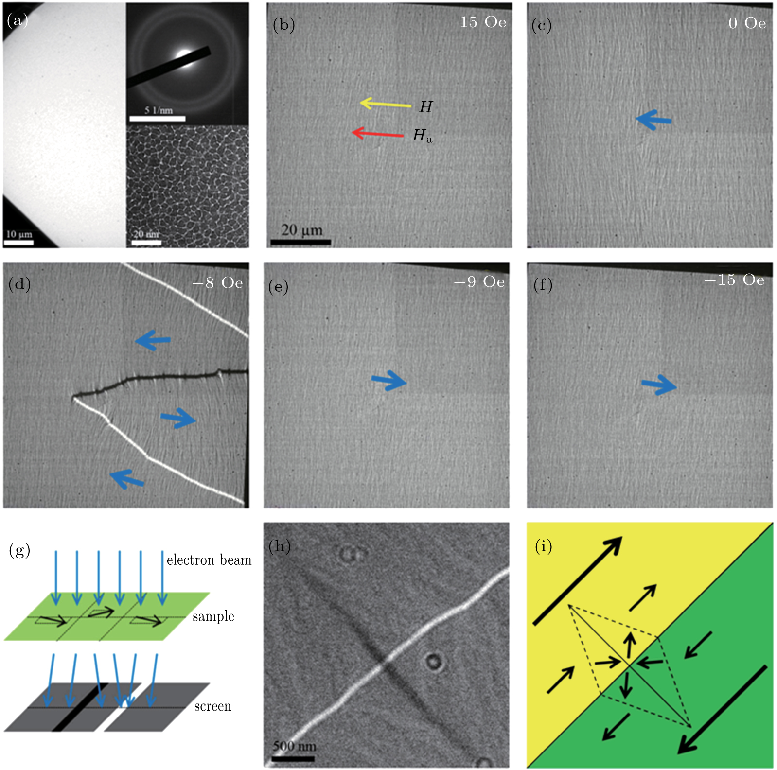
Figure 2(a) shows the TEM image of sample A. In this figure the diffused rings in the selected area diffraction pattern (SADP, inset) confirm that the CoFeB alloy film is of the amorphous phase. The high spatial resolution image (inset) shows a granular microstructure, which indicates the presence of element segregation on a several-nanometer scale. Though the detailed microstructure and chemical composition have not been clarified, the existence of nonuniform magnetic intrinsic properties due to microstructure in the sample is anticipated. The domain dynamic process in in-situ observation is shown in Figs. 2(b)–2(f), which correspond to points b–f on the loop of sample A in Fig. 1, respectively. As a magnetic field is used in sputtering process, a uniaxial anisotropy is induced as indicated by the red arrow in Fig. 2(b). It is clearly shown that ripple domains are uniformly distributed in the film plane (Figs. 2(b)–2(f)) and the ripple directions are all perpendicular to the uniaxial anisotropy direction. The ripple domain is a kind of typical domain structure in the soft magnetic thin film,[18] which is caused by local disturbance of in-plane magnetization as schematically shown in Fig. 2(g). In the case of nanocrytalline materials such as permalloy the disturbance of the magnetization vector is ascribed to the dispersion of anisotropy constant in each crystalline grain.[19] In the amorphous CoFeB of this work, the dispersed anisotropy is considered to be caused by the variable shape and composition of the cluster as shown in Fig. 2(a), which makes the magnetization direction fluctuate with the direction of the induced uniaxial anisotropy. When the field is 15 Oe (Fig. 2(b)) along the direction of anisotropy, the ripple contrast is weak. However, with the field decreasing to zero (Fig. 2(c)), the ripple contrasts become stronger. As the field further increases close to the coercivity (−8 Oe), the reverse domains emerge and the domain wall moves quickly through the specimen within a field range of 1.0 Oe, and one of the images in this dynamic process is shown in Fig. 2(d). The ripple contrast becomes stronger than the remanent state but the ripple direction is fixed, which means that the local magnetization disturbance becomes more drastic while the mean magnetization direction does not change, which is parallel or antiparallel to the field direction. The domain walls marked as white and black lines are 180-degree walls and their magnetization directions in domain are indicated by blue arrows. In the reversal process, the 180° magnetic domain wall is zigzag-like on a several-micron scale. A kind of cross-tie domain wall is found, whose magnified image and spin structure are shown in Figs. 2(h) and 2(i), respectively. This structure has lower energy than the 180° Néel wall because it consists mainly of energetically favorable 90° walls.[20] When the field decreases to −9 Oe (Fig. 2(e)) and −15 Oe (Fig. 2(f)) separately, the ripple contrast becomes weaker and weaker, indicating that the magnetization is gradually inversely saturated. Figure 2 shows the magnetization reversal process of single soft ferromagnetic thin film, i.e., the reverse domain nucleates somewhere, generally at the positions with large demagnetization field, and expands through domain wall movement.
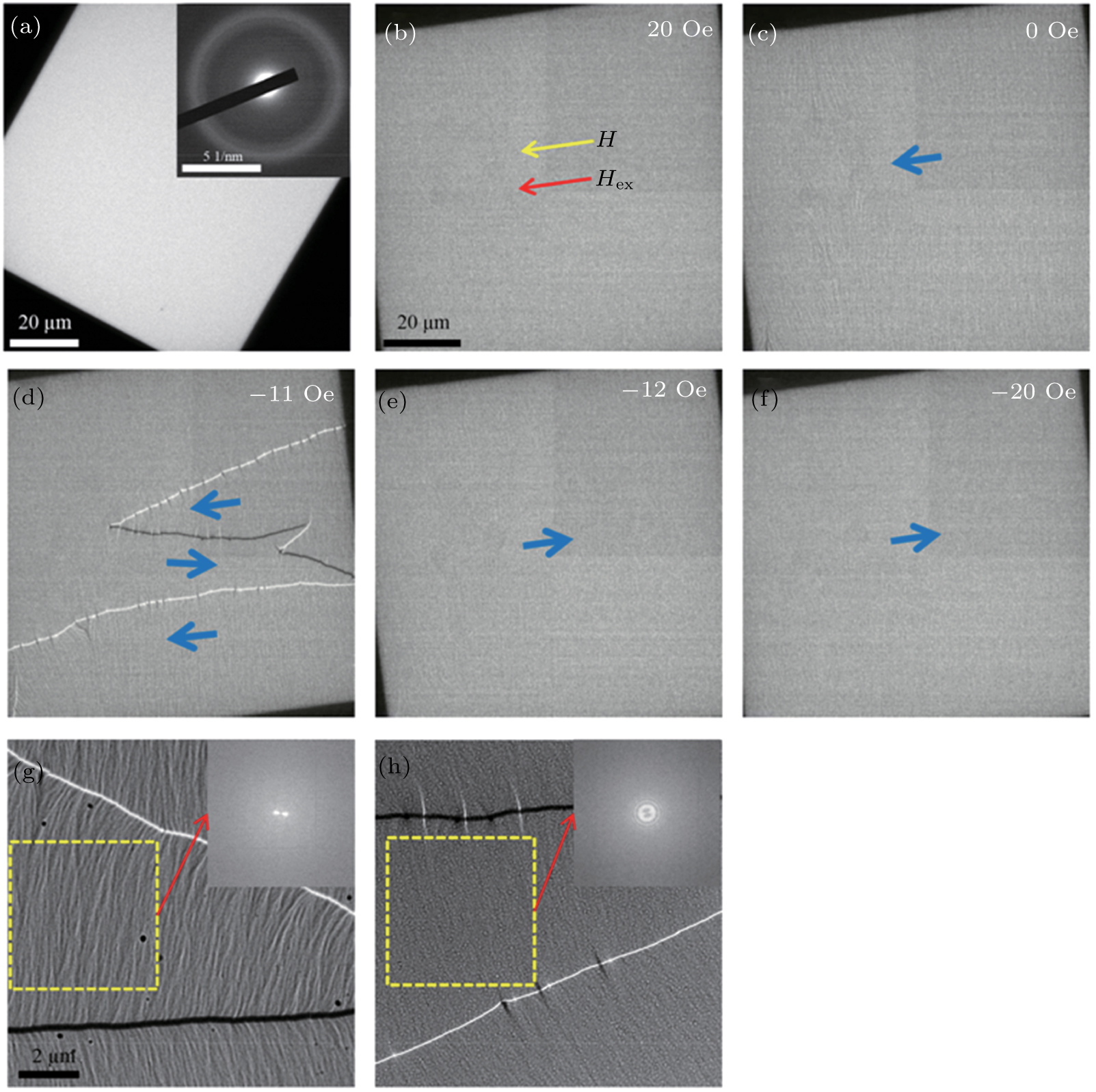
The microstructure of sample B is shown in Fig. 3(a), with no distinct difference in the bright field image in comparison with that of sample A. However, the SADP of sample B shows one additional diffused ring which corresponds to the IrMn (110) lattice plane between two diffused rings of sample A, indicating that the IrMn layer is amorphous. The amorphous IrMn phase cannot form the large range uncompensated spin structure at the interface, thus the macroscopic EB phenomenon is hardly found (less than 1 Oe). The in-situ magnetization reversal process of sample B is shown in Figs. 3(b)–3(f), which correspond to points b–f on the loop of sample B in Fig. 1, respectively. In general, the reversal process is quite similar to that of sample A, but the magnetization reversal and wall movement occur at the coercivity −11 Oe (Fig. 3(d)), and the contrast of ripple domains is much weaker than that of sample A throughout the magnetization process. For comparison, high magnified domain images at the coercivities of samples A and B are shown in Figs. 3(g) and 3(h), respectively. Fast Fourier transform (FFT) is applied to the yellow box areas and shown in the insets. It can be clearly confirmed that the magnetic disturbance of CoFeB/IrMn (5 nm) bilayer is much weaker than that of CoFeB single layer. Furthermore, the domain wall width in the bilayer is obviously narrower than that in the single layer. Both phenomena are considered to be caused by the exchange bias coupling between FM and AFM layer, which increases the effective anisotropy field of CoFeB. This leads to degradation of the local magnetization fluctuation, and reduces the wall width as well, since the wall width is reversely proportional to the effective anisotropy constant.
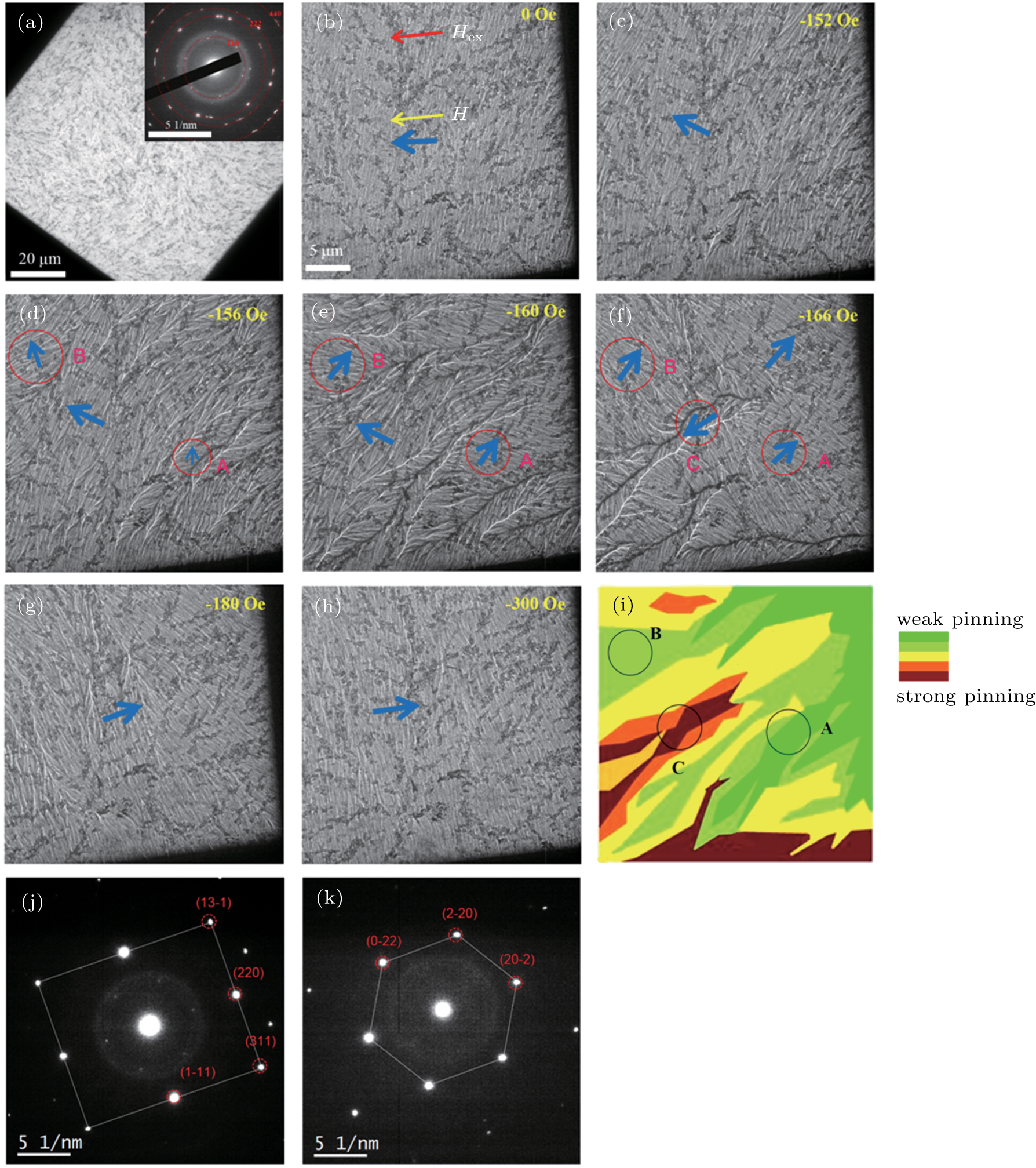
The microstructure and domain structure for sample C are quite different from those of samples A and B. The bright field image of sample C (Fig. 4(a)) shows the obvious diffraction contrast from the IrMn layer with a thickness of 30 nm. From the SADP shown in the insert of Fig. 4(a), the IrMn layer is polycrystalline. The in-situ experimental results are shown in Figs. 4(b)–4(h), which correspond to points b-h on the loop of sample C in Fig. 1, respectively. The magnetic reversal process is much more complicated than those of the other two samples. In Fig. 4(b) when the field is 0 Oe, there exists a weak ripple with the direction perpendicular to the EB direction. As the field decreases to −152 Oe (Fig. 4(c)), the ripple contrasts become a little stronger and the directions rotate a small angle, which means that the mean magnetization direction uniformly rotates. When the field decreases to −156 Oe (Fig. 4(d)), the ripple contrasts become quite strong, indicating that there is a violent magnetization fluctuation due to the competition between the external field and the exchange bias field. At the same time, the ripple direction in the red circle area A rotates a large angle, and that in area B rotates a small angle, which means that the pinning forces in the two areas are weaker than those in any other areas. As the field decreases from −160 Oe to −166 Oe, the magnetization rotations occur, which are larger in areas A and B as indicated by the blue arrows in Figs. 4(e) and 4(f). In this stage, the reversed domains also form high contrast domain walls and wall shifts are observed, but the magnetization in area C has not been reversed yet. As field deceases to −180 Oe, the ripple contrasts keep unchanged, and with the field decreasing to −300 Oe the sample magnetization uniformly rotates to the exchange bias direction.
According to the dynamic domain structures, we make a mapping to demonstrate the sequence of the magnetization reversal as shown in Fig. 4(i). Though the magnetostatic interaction among domains should be considered, the map may present the distribution of pinning force in the sample. It is shown that the pinning effect is clearly not uniform and only about 1/6 of the area exhibits the pinning effect, which is in qualitative agreement with the result of XMLD.[8] Furthermore, the SADPs in the two selected areas A and C in Figs. 4(j) and 4(k) show that the crystal orientations are different. The crystal zone axis of area A is
 and that of area C is
 . According to a previous report, the IrMn (111) crystal face has the highest spin density in all crystal faces, thus the bias field in IrMn (111) texture is the largest.[21] This should be one of the reasons why area C has a larger pinning force than area A as shown in the experiment.
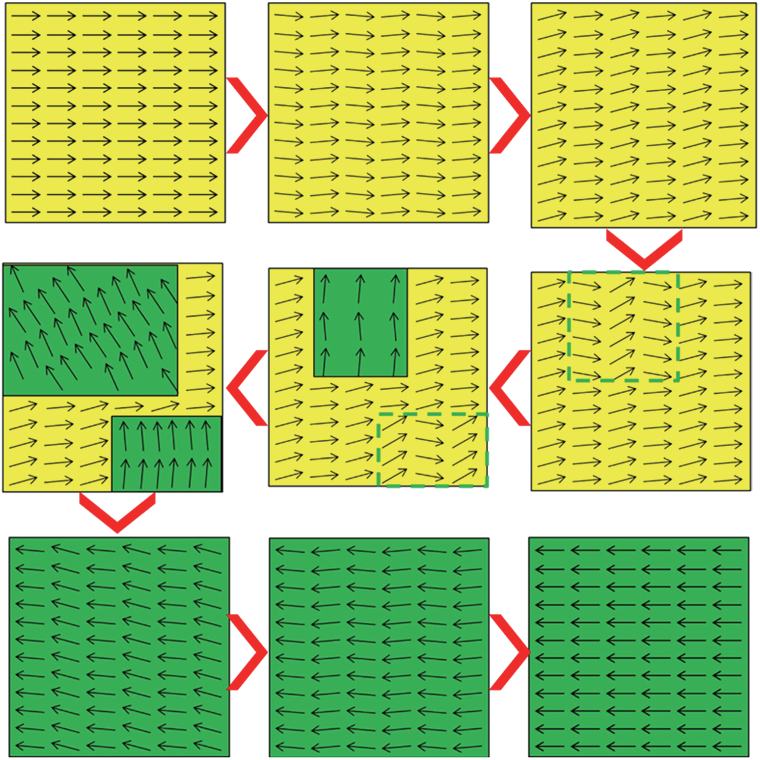
The magnetic reversal model of sample C is summarized in Fig. 5. In this figure the magnetization of FM layer rotates uniformly at the beginning of the decrease in the external field, and also at the final stage before the magnetization is saturated. This indicates that there is no difference in the pinning force from AFM at the two stages. However, with the field close to the coercivity point, the inhomogeneous magnetization reversal indicates that the pinning force is not uniformly distributed. Our observation results quite agree with the micromagnetic simulation results,[22] where they supposed that a certain percentage of ferromagnetic spins are pinned by the AFM layer and the pinning area is nonuniformly distributed. As proposed in Malozemoffʼs papers,[5,23] the nonuniform pinning effect distribution is responsible for the difference between experimental and theoretical bias field values. The crystallinity of AFM can strongly influence the EB field. Further, the roughness of interface can create the areas with both the opposite AFM uncompensated spin orientations and the compensated spin structures, which destroys the uniform pinning and reduces the magnitude of the EB field. The characterization of interface roughness on a several atomic layer scale is not so easy, and further analysis is under preparation.

