Effect of depositing PCBM on perovskite-based metal–oxide–semiconductor field effect transistors
Luan Su-Zhen1, Wang Yu-Cheng2, Liu Yin-Tao2, Jia Ren-Xu2, †
School of Electronic Engineering, Xidian University, Xi’an 710071, China
School of Microelectronics, Xidian University, Xi’an 710071, China


† Corresponding author. E-mail: rxjia@mail.xidian.edu.cn

Abstract

In this manuscript, the perovskite-based metal–oxide–semiconductor field effect transistors (MOSFETs) with phenyl-C61-butyric acid methylester (PCBM) layers are studied. The MOSFETs are fabricated on perovskites, and characterized by photoluminescence spectra (PL), x-ray diffraction (XRD), and x-ray photoelectron spectroscopy (XPS). With PCBM layers, the current–voltage hysteresis phenomenon is effetely inhibited, and both the transfer and output current values increase. The band energy diagrams are proposed, which indicate that the electrons are transferred into the PCBM layer, resulting in the increase of photocurrent. The electron mobility and hole mobility are extracted from the transfer curves, which are about one order of magnitude as large as those of PCBM deposited, which is the reason why the electrons are transferred into the PCBM layer and the holes are still in the perovskites, and the effects of ionized impurity scattering on carrier transport become smaller.

PACS: ;72.40.+w;;78.55.Kz;
1. Introduction

As a potential photoelectric material, organic–inorganic halide perovskite (OIHP) has drawn tremendous attention in the past several years.[15] Perovskites in the form of ABX3 (A = methylammonium, B = lead, X = chlorine, bromine, and iodine) exhibit excellent properties such as long electron diffusion lengths, the ability to strongly absorb light, and extremely low preparation cost.[68] The power conversion efficiency of the OIHP based solar cells has increased from 3.8% in 2009 to 21% in 2016.[912] Perovskite based photovoltaic devices, such as photodetectors, lasers, and phototransistors have been widely analyzed in recent years.[1318] However, OIHPs are not applied to industrial production since the film can be easily decomposed in the air, and the mobile ions like iodine and methylammonium+ will affect the stability and reliability of the photovoltaic device.[12,19,20]

The study of the ion migration in the OIHP film focused on how the ions move and how the ions inhibit.[21,22] Yang et al.[20] and Xu et al.[23] performed the density functional theory calculations of both the diffusion barriers and the formation energies for MA+, I, and Pb2+. They found that the I and MA+ have lower diffusion barriers than the Pb2+.[20,23] The phenyl-C61-butyric acid methylester (PCBM) was often used for the inhibition of the iodine ions.[24] Liu et al. proposed a new model based on the hindering theory of ions (vacancies) migration with PCBM.[19] Xu et al. proved that the PCBM phase promotes electron extraction and passivates the key antisite defects.[23] In many reports the PCBM has been analyzed on devices such as solar cells and photodetectors.[2427] The perovskite based phototransistors with and without the PCBM layer are also quite significant. However, the latest literature focuses on the perovskite field-effect transistors under different temperatures without the PCBM layer.[28,29]

In the present study, the structures (#1: perovskite, #2: PCBM/perovskite/PCBM) of OIHP-based phototransistors are prepared and discussed. The perovskite films are characterized by photoluminescence spectra (PL), x-ray diffraction (XRD) and x-ray photoelectron spectroscopy (XPS). Current–voltage (IV) curves are measured and the channel carrier mobility is calculated. The effects of the PCBM layers on the perovskite MOS field-effect transistors are presented by energy band and transport loops diagrams.

2. Experimental details and results

The 400- , heavily doped Si ( ) with 300-nm SiO2 oxide layers were prepared as the substrate and the oxide layer, respectively. Methylammonium iodide (MAI) was synthesized by stoichiometrically reacting methylamine with hydroiodic acid. The precursor was prepared by mixing MAI and PbCl2 in a molar ratio of 3:1 in N, N-dimethylformamide (DMF). The mixed solution was then spin-coated on the Si/SiO2 substrate at 2000 rpm for 30 s. Phenyl-C61-butyric acid methylester (PCBM, Nichem Fine Technology Co., Ltd.) was spin coated after and/or before the perovskite layer at 1500 rpm for 30 s, and the samples were annealed at 90 °C for 30 min. Aluminum and gold were used as the back and positive electrode by magnetron sputtering, respectively. The area of the gate electrode is , and the channel length is . The structures for the MOSFETs are shown in Fig. 1.

Fig. 1. (color online) Structures for MOSFETs (#1) Au/perovskite/SiO2/Si/Al and (#2) Au/PCBM/perovskite/PCBM/SiO2/Si/Al.

The XRD, XPS, and PL measurements are presented in Fig. 2. The x-ray diffraction spectrum (Bruker D9 advance diffractometer, Cu–Kα radiation) is shown Fig. 2(a). It is found that the perovskite film has a highly oriented crystal domain with the long axis preferentially oriented parallel to the substrate. Peaks at 14.2°, 28.5° are assigned to the (110) and (220) planes of crystalline CH3NH3PbI3−xClx, respectively.[30] The x-ray photoelectron spectroscopy (Thermo Fisher Scientific ESCALAB 250 system, Al–Kα) is conducted in the case without ion etching. The elements (and corresponding binding energies) in the examining spectrum (in Fig. 2(b)) are obtained to be Pb 4f (145 eV), C 1s (285 eV), N 1s (416 eV), and I 3d (621 eV), respectively. The double peaks of Pb and I are the main peaks and the satellite peaks (shown in Fig. 2(c)).[31] Figure 2(d) shows the photoluminescence spectrum, and the photoluminescence peak at 780 nm is consistent with previously reported results.[32]

Fig. 2. (a) X-ray diffraction (XRD), ((b) and (c)) x-ray photoelectron spectroscopy (XPS) results, and (d) photoluminescence spectrum (PL) measurements for the perovskite films deposited on the Si/SiO2 substrate.

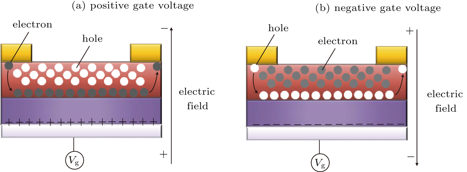
The transfer characteristic curves of the transistors, measured in the dark, are shown in Figs. 3(a) and 3(b) and those measured under illumination are displayed in Figs. 3(c) and 3(d). It is found that the primordial perovskite based field-effect transistor shows current values less than 10−10 A at 20-V gate voltage in the dark, and less than 10−8 A at 20-V gate voltage under illumination, respectively. However, the values of current increase when PCBM layers are deposited on both sides. Since PCBM is widely used as an electron transport layer,[33,34] depositing PCBM near the oxide layer can conduce to the accumulation of the electrons, while PCBM away from the oxide layer will resist the accumulation of electrons (shown in Fig. 4). In the dark, the electrical hysteresis by positive and negative sweep disappears with PCBM layers due to the suppression of ions drifting. As in the light condition, the number of photo-generated carriers is much bigger than that of ions, thus the positive and negative current curves coincide and the hysteresis caused by ions is ignored. Since perovskite is a weak p-type semiconductor, the MOS transistors are bipolar transistors,[35,36] which means the transistors work under both positive and negative voltages. When positive gate voltage is applied, electrons accumulate near the SiO2/perovskite (#1 and #2) or SiO2/PCBM (#3) interface (shown in Fig. 4), while holes are pulled away from the interface and distributed in the perovskite or PCBM film. In this case, the electrons play a main role in the current transport. Similarly, the holes will primarily affect the current transport when negative gate voltage is applied.

Fig. 3. Drain current–gate voltage curves at Vd = -5 V in ((a) and (b)) the dark and ((c) and (d)) light condition.
Fig. 4. (color online) Energy band diagrams of transistors (a) #1 Au/perovskite/SiO2/Si/Al (b) #2 Au/PCBM/perovskite/PCBM/SiO2/Si/Al. Ec, Ev, EF, Ecpcbm, Evpcbm, Eco, Evo, EFAl, and EFAu are the conduction band, valance band, Fermi level of perovskite, PCBM, SiO2 layer, and metal electrode, respectively. The black and white balls are symbolized as electrons and holes, respectively.

The output current curves in the dark and under illumination (2 mW/cm2) are illustrated in Figs. 5(a) and 5(b). After PCBM deposited on both sides of the perovskite film, the hysteresis of output current is eliminated as shown in Fig. 3. Since the output current is not saturated, the channel mobility can be extracted from the following equation for the linear region:

where W, L, C, μ, Vt are the channel width, the channel length, the gate capacitance per unit area, the field effect mobility, and the threshold voltage, respectively. The width of the electrode is , the channel length is , and the capacitance of the oxide layer per unit area is . Since the variations of current curves are linear, the parameter can be ignored in Eq. (1). The charge transport loops under positive and negative gate voltage are illustrated in Figs. 6(a) and 6(b). When positive gate voltage is applied, electrons accumulate near the interface, and thus the channel mobility of electrons can be obtained. Likewise, the hole channel mobility can be obtained by fitting the transfer current curves under negative gate voltage as seen in Fig. 6(b). By fitting the curves in Fig. 3, the channel mobilities under light condition are calculated. For transistor 1, the values of electron and hole gate mobility are and , respectively. With PCBM layers deposited in MOSFET, the electrons are transferred into the PCBM layer and the holes are still in the perovskites, and the effect of ionized impurity scattering on carrier transport becomes smaller. The electron mobility and hole mobility are, respectively, and , which are an order of magnitude larger than that in the case without PCBM.

Fig. 5. (color online) Drain current–drain voltage curves with different gate voltages (Vg = 30 V and −30 V) for transistors (a) Au/perovskite/SiO2/Si/Al and (b) Au/PCBM/perovskite/PCBM/SiO2/Si/Al in the dark and under illumination (2 mW/cm2).
Fig. 6. (color online) Charge transport loops under (a) positive and (b) negative gate voltages under light condition.
3. Conclusions

In this study, the effects of perovskite based MOSFETs with and without PCBM are discussed. With PCBM layers, the current–voltage hysteresis phenomenon is effetely reduced, and both the transfer and output current values increase. The band energy diagrams are proposed, which indicate that the electrons are transferred into the PCBM layer, resulting in the increase of photocurrent. By fitting the MOSFETs transfer curves, the values of electron and hole gate mobility under light condition are calculated. With PCBM layers deposited in MOSFET, the electrons are transferred into the PCBM layer and the holes are still in the perovskites, and the effects of ionized impurity scattering on carrier transport become smaller. The electron mobility and hole mobility are, respectively, and , which are an order of magnitude larger than in the case without PCBM.

Reference
1 Noel N K Habisreutinger S N Wenger B Klug M T Hörantner M T Johnston M B Nicholas R J Moore D T Snaith H J 2017 Energy Environ. Sci. 10 145
2 Ma F Li J Li W Lin N Wang L Qiao J 2017 Chem. Sci. 8 800
3 Liu K Yao Y Wang J Zhu L Sun M Ren B Xie L Luo Y Meng Q Zhan X 2017 Mater. Chem. Front. 1 100
4 Zhuang S W Xu J X Wu B Zhang Y T Dong X Li G X Zhang B L Du G T 2017 Chin. Phys. 26 017802
5 Erum N Iqbal M A 2017 Chin. Phys. 26 047102
6 Qin T Huang W Kim J E Vak D Forsyth C McNeill C R Cheng Y B 2017 Nano Energy 31 210
7 Zhu H Trinh M T Wang J Fu Y Joshi P P Miyata K Jin S Zhu X Y 2017 Adv. Mater 29 1603072
8 Yang I S Sohn M R Sung S D Kim Y J Yoo Y J Kim J Lee W I 2017 Nano Energy 32 414
9 Saliba M Matsui T Seo J Y Domanski K Correa-Baena J P Nazeeruddin M K Zakeeruddin S M Tress W Abate A Hagfeldt A Gratzel M 2016 Energy Environ. Sci. 9 1989
10 Kojima A Teshima K Shirai Y Miyasaka T 2009 J. Am. Chem. Soc. 131 6050
11 Heo J H Song D H Im S H 2014 Adv. Mater. 26 8179
12 Jung H S Park N G 2015 Small 11 10
13 Liu X Wang C Lyu L Wang C Xiao Z Bi C Huang J Gao Y 2015 Phys. Chem. Chem. Phys. 17 896
14 Saidaminov M I Adinolfi V Comin R Abdelhady A L Peng W Dursun I Yuan M Hoogland S Sargent E H Bakr O M 2015 Nat. Commun. 6 8724
15 Chen J Zhou S Jin S Li H Zhai T 2016 J. Mater. Chem. 4 11
16 Ramasamy P Lim D H Kim B Lee S H Lee M S Lee J S 2016 Chem. Commun. (Camb) 52 2067
17 Zhu H Fu Y Meng F Wu X Gong Z Ding Q Gustafsson M V Trinh M T Jin S Zhu X Y 2015 Nat. Mater 14 636
18 Liang Y Yao Y Zhang X Hsu W L Gong Y Shin J Wachsman E D Dagenais M Takeuchi I 2016 AIP Adv. 6 015001
19 Liu Y T Jia R X Wang Y C Hu Z Y Zhang Y M Pang T Q Zhu Y J Luan S Z 2017 ACS Appl. Mater. Inter. 9 15638
20 Yang D Ming W Shi H Zhang L Du M H 2016 Chem. Mater. 28 4349
21 Chen B Yang M Zheng X Wu C Li W Yan Y Bisquert J Garcia-Belmonte G Zhu K Priya S 2015 J. Phys. Chem. Lett. 6 4693
22 Eames C Frost J M Barnes P R O’Regan B C Walsh A Islam M S 2015 Nat. Commun. 6 7497
23 Xu J Buin A Ip A H Li W Voznyy O Comin R Yuan M Jeon S Ning Z McDowell J J Kanjanaboos P Sun J P Lan X Quan L N Kim D H Hill I G Maksymovych P Sargent E H 2015 Nat. Commun. 6 7081
24 Liu X Yu H Yan L Dong Q Wan Q Zhou Y Song B Li Y 2015 ACS Appl. Mater. Inter. 7 6230
25 Jeng J Y Chen K C Chiang T Y Lin P Y Tsai T D Chang Y C Guo T F Chen P Wen T C Hsu Y J 2014 Adv. Mater. 26 4107
26 Bai Y Yu H Zhu Z Jiang K Zhang T Zhao N Yang S Yan H 2015 J. Mater. Chem. 3 9098
27 Chin X Y Cortecchia D Yin J Bruno A Soci C 2015 Nat. Commun. 6 7383
28 Kuang C Tang G Jiu T Yang H Liu H Li B Luo W Li X Zhang W Lu F Fang J Li Y 2015 Nano Lett. 15 2756
29 Labram J G Fabini D H Perry E E Lehner A J Wang H Glaudell A M Wu G Evans H Buck D Cotta R Echegoyen L Wudl F Seshadri R Chabinyc M L 2015 J. Phys. Chem. Lett. 6 3565
30 Adhikari N Dubey A Khatiwada D Mitul A F Wang Q Venkatesan S Iefanova A Zai J Qian X Kumar M Qiao Q 2015 ACS Appl. Mater. Inter. 7 26445
31 Kumar G R Savariraj A D Karthick S N Selvam S Balamuralitharan B Kim H J Viswanathan K Vijaykumar K M Prabakar K 2016 Phys. Chem. Chem. Phys. 18 7284
32 Liu D Yang J Kelly T L 2014 J. Am. Chem. Soc. 136 17116
33 Trifiletti V Roiati V Colella S Giannuzzi R Marco L D Rizzo A Manca M Listorti A Gigli G 2015 ACS Appl. Mater. Inter. 7 4283
34 Kim S S Bae S Jo W H 2015 Chem. Commun. 51 17413
35 Li F Ma C Wang H Hu W Yu W Sheikh A D Wu T 2015 Nat. Commun. 6 8238
36 Wang Q Shao Y Xie H Lyu L Liu X Gao Y Huang J 2014 Appl. Phys. Lett. 105 163508