


High mobility ultrathin ZnO p–n homojunction modulated by Zn0.85Mg0.15O quantum barriers
Cite this Article
Yang Jing-Jing, Fang Qing-Qing, Du Wen-Han, Zhang Ke-Ke, Dong Da-Shun. High mobility ultrathin ZnO p–n homojunction modulated by Zn0.85Mg0.15O quantum barriers. Chinese Physics B, 2018, 27(3): 037804 
Permissions
High mobility ultrathin ZnO p–n homojunction modulated by Zn0.85Mg0.15O quantum barriers
† Corresponding author. E-mail:
Abstract
The adding of ZnMgO asymmetric double barriers (ADB) in p-ZnO: (Li, N)/n-ZnO homojunction affects the p–n junction device performance prominently. Two different homojunctions are fabricated on Si (100) substrates by pulsed laser deposition; one is the traditional p-ZnO: (Li, N)/n-ZnO homojunction with different thicknesses named as S1 (250 nm) and S2 (500 nm), the other is the one with ADB embedded in the n-layer named as Q (265 nm). From the photoluminescence spectra, defect luminescence present in the S-series devices is effectively limited in the Q device. The current–voltage curve of the Q device shows Zener-diode rectification property because the two-dimensional electron gas tunnels through the narrow ZnMgO barrier under a reverse bias, thus decreasing the working p–n homojunction thickness from 500 nm to 265 nm. The ADB-modified homojunction shows higher carrier mobility in the Q device. The electroluminescence of the ZnO homojunction is improved in Q compared to S2, because the holes in p-type ZnO (Li, N) can cross the wide ZnMgO barrier under a forward bias voltage into the ZnO quantum well. Therefore, electron–hole recombination occurs in the narrow bandgap of n-type ZnO, creating an ultraviolet light-emitting diode using the ZnO homojunction.
1. Introduction
ZnO is a wide band gap transparent II–VI semiconductor. It may be highly significant in future device applications.[1–8] Great efforts have been devoted to creating light-emitting diodes[9] and laser diodes[10–12] using ZnO. Band-gap engineering is used to create heterojunctions and quantum well structures (QWS) with matching material properties.[13] However, developing electrically pumped ZnO p–n junction devices is difficult because of the lack of reliable and controllable p-type ZnO.[14] Appropriate rectifying characteristics can be successfully achieved when the ZnO p–n junction thickness approaches micrometer-scale.[15] The transparent nature of ZnO p–n junctions permits their application in solar cell devices.[16] If the device thickness can be reduced, the transmittance in the wavelength range of the visible spectrum may be improved,[17] and applications using flexible substrates could be facilitated.[17–19] Therefore, maintaining device performance while reducing device thickness is an important development direction.
Previously, we have reported antimony (Li, N)-doped p-type ZnO[20] prepared by pulsed laser deposition. In this work, ZnO/ZnMgO asymmetric double barriers (ADB) are embedded to improve the performance of the ZnO p–n homojunction. Two different types of p-type/n-type ZnO homojunctions are prepared by pulsed laser deposition (PLD) on Si substrates. The ZnO p–n homojunctions use ZnO: (Li, N) and pure ZnO as the p- and n-layers, respectively; meanwhile, the Q ZnO p–n homojunctions have ZnO/ZnMgO ADB embedded in the n-type ZnO layer.
2. Material and methods
ADB structures in ZnO p–n homojunction were fabricated on Si substrates by pulse laser deposition. In order to determine whether the ADB functions well or not in the ZnO homojunction at RT, the ZnO/Zn0.85Mg0.15O ADB, S-series p-ZnO: (Li, N)/n-ZnO homojunction, and Q p-ZnO: (Li, N)/ADB/n-ZnO homojunction were prepared by PLD separately.
The ZnO/Zn0.85Mg0.15O ADB was deposited on Si(100) substrates, while the other ZnO homojunctions were deposited on Si(100) substrates using a KrF excimer laser (λ = 248 nm, full width at half-maximum FWHM = 30 ns). The energy of the laser was 190 mJ/pulse, and the pulse frequency was 4 Hz. ZnO, Zn0.9Li0.1O, and Zn0.85Mg0.15O targets were synthesized from high-purity ZnO, MgO, and Li2O (99.999%) powders, which were ceramic-pressed and sintered at 1050 °C for 12 h in flowing air. The doping N2 pressure was 2.3 Pa, and the growth temperature was 450 °C. The structure of ZnO/Zn0.85Mg0.15O ADB is shown in Fig.
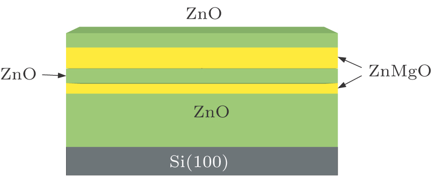 | Fig. 1. (color online) Geometric structure of ZnO/Zn0.85Mg0.15O ADB. |
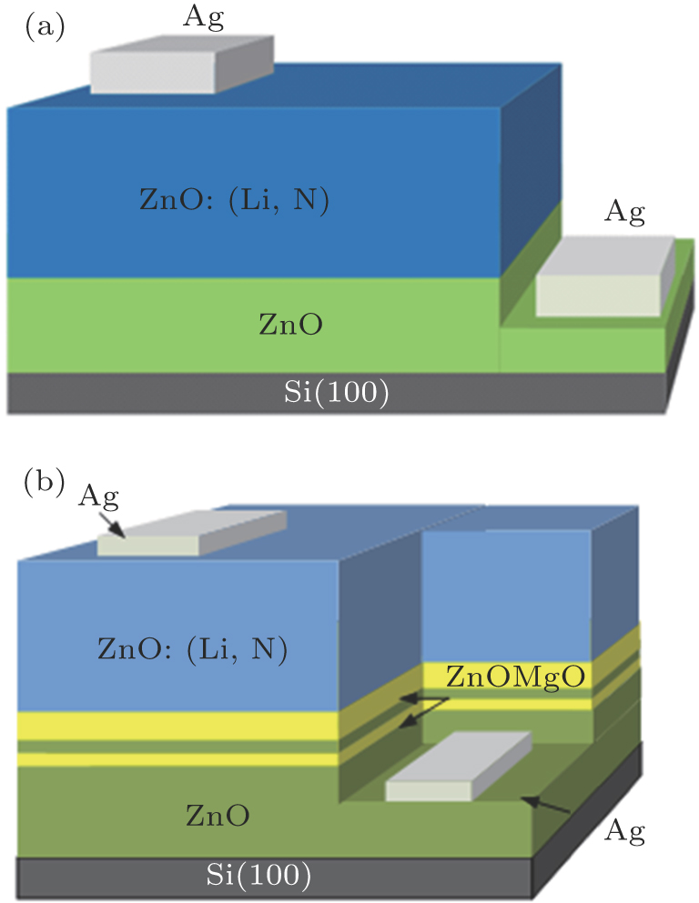
 | Fig. 2. (color online) Geometric structures of ZnO p–n junctions with or without ZnMgO ADB: (a) S-series p–n junctions without ZnMgO ADB; (b) Q p–n junctions with ZnMgO ADB. |
As shown in Fig.
| Table 1.
Thickness information of ZnO/Zn0.85Mg0.15O ADB. . |
| Table 2.
Thickness information of different ZnO p–n homojunctions. . |
3. Results and discussion
3.1. Structure measurements
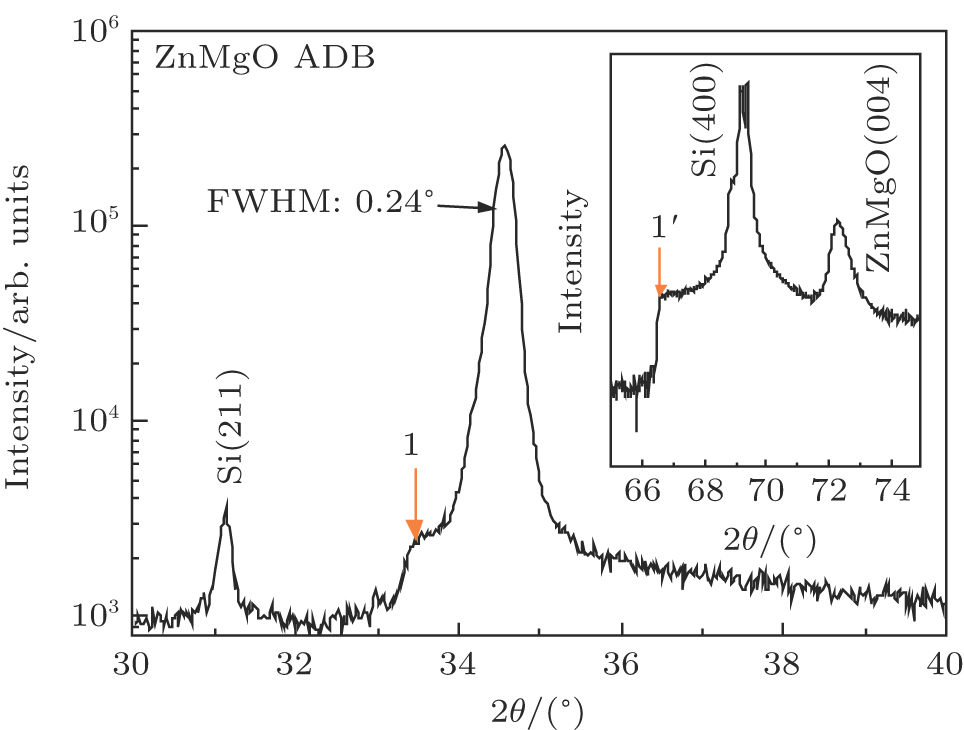
Figure
 | Fig. 3. (color online) XRD pattern of ZnO/Zn0.85Mg0.15O ADB thin film on Si(100) substrate. Inset shows the XRD pattern at a different diffraction angle range of the same sample. The arrows marked with 1 and 1′ indicate the similarity of ZnMgO(002) and Si(400) XRD peak shapes. |
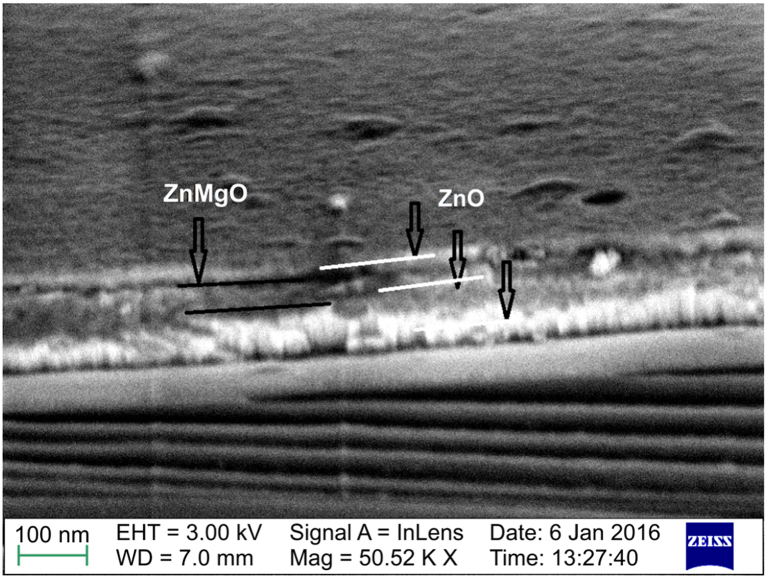 | Fig. 4. (color online) Cross-section SEM image of ZnO/Zn0.85Mg0.15O ADB thin film on silicon substrate. |
Next, we inserted the ZnO/Zn0.85Mg0.15O ADB in S-series p-ZnO: (Li, N)/n-ZnO homojunction and tested the optical properties of the resulting Q-series p-ZnO: (Li, N)/ADB/n-ZnO homojunction to confirm the realization of quantum effects.
3.2. Luminescence properties
In order to investigate the influence of the ADB on the performance of the homojunction, the photoluminescence spectra were obtained at RT using 325-nm laser light. Figure
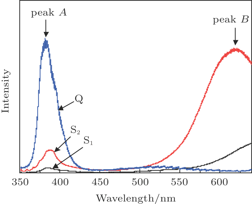 | Fig. 5. (color online) Photoluminescence spectra of S1, S2, and Q. |
3.3. Electrical properties
3.3.1. Current–voltage curve
In order to confirm the modulation by the added ADB structure, we tested the current–voltage (I–V) properties of all ZnO p–n homojunctions. All I–V measurements were performed using a Keithley 2611A source meter.
Figure
 | Fig. 6. (color online) I–V curves of ZnO p–n homojunctions with different conditions on Si substrates. |
The Q device exhibits obvious Zener breakdown features while sample S2 does not. It is known that, for 
3.3.2. Hall-effect
To determine how the ADB influences the electron mobility of the 2DEG, we performed Hall-effect measurements with electrodes shown in Fig.
 | Fig. 7. The four-probe method used for Hall effect test. |
| Table 3.
Electrical properties of ZnO: (Li, N)/ADB/ZnO thin films. . |
The electrical properties were measured in the Q device under 0.1 T magnetic field to determine the carrier density and mobility. The Hall mobility μ in the Q device is much higher than that in the S-series devices, and the resistivity of the Q sample is reduced to 

3.4. Electroluminescence of ZnO: (Li, N)/ADB/ZnO p–n homojunction
Electroluminescence (EL) characterizations were performed to determine the luminescence properties of S2 and Q p–n homojunctions. A monochromator (ARSSP2557) was used to collect the emission and EL spectra.
Figure 

 | Fig. 8. (color online) Electroluminescence spectra of S2 and Q ZnO homojunctions. |
The carrier transport mechanism of the Q homojunction is shown schematically in Fig.
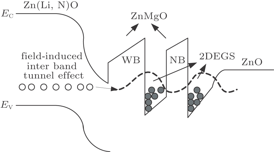 | Fig. 9. The carrier transport schematic diagram of field-induced inter band tunnel effect of ADB-added ZnO p–n homojunction. |
4. Conclusion
A Zn0.85Mg0.15O ADB structure is added into the p-ZnO: (Li, N)/n-ZnO p–n homojunction to study the effects of the ADB on the junction performance. The Zn0.85Mg0.15O ADB shows a modulation effect in the ZnO p–n homojunction at RT. For unmodified wide-band-gap semiconductors, such as ZnO, the electron tunnelling probability is very low, which greatly reduces the quantum efficiency. However, we find that the adding of Zn0.85Mg0.15O ADB enhances the performance of the p–n homojunction in ultrathin films (265 nm) effectively, and a field-induced inter-band tunnelling effect in the ZnO: (Li, N)/ZnO p–n homojunction is observed under very small reverse bias voltages facilitated by the ADB design. Furthermore, the ZnO p–n homojunction with ZnMgO ADB has stronger exciton recombination efficiencies than the ZnO p–n homojunction without ZnMgO ADB, exhibiting UV-wavelength light-emitting characteristics at lower thicknesses and higher Hall mobility. This means that the adding of ZnMgO ADB structures in ZnO homojunction can greatly improve the performance of the ultrathin ZnO p–n homojunction. The device modification demonstrates increased performance in both rectifying characteristics and EL properties.
Reference
| [1] | |
| [2] | |
| [3] | |
| [4] | |
| [5] | |
| [6] | |
| [7] | |
| [8] | |
| [9] | |
| [10] | |
| [11] | |
| [12] | |
| [13] | |
| [14] | |
| [15] | |
| [16] | |
| [17] | |
| [18] | |
| [19] | |
| [20] | |
| [21] | |
| [22] | |
| [23] | |
| [24] | |
| [25] | |
| [26] | |
| [27] |