Enhanced radiation-induced narrow channel effects in 0.13- μ m PDSOI nMOSFETs with shallow trench isolation
Zhang Meng-Ying1, 2, †, Hu Zhi-Yuan1, Bi Da-Wei1, Dai Li-Hua1, 2, Zhang Zheng-Xuan1
State Key Laboratory of Functional Materials for Informatics, Shanghai Institute of Microsystem and Information Technology, Chinese Academy of Sciences, Shanghai 200050, China
University of Chinese Academy of Sciences, Beijing 100049, China


† Corresponding author. E-mail: myzhang@mail.sim.ac.cn

Abstract

Total ionizing dose responses of different transistor geometries after being irradiated by 60Co γ-rays, in 0.13- partially-depleted silicon-on-insulator (PD SOI) technology are investigated. The negative threshold voltage shift in an n-type metal-oxide semiconductor field effect transistor (nMOSFET) is inversely proportional to the channel width due to radiation-induced charges trapped in trench oxide, which is called the radiation-induced narrow channel effect (RINCE). The analysis based on a charge sharing model and three-dimensional technology computer aided design (TCAD) simulations demonstrate that phenomenon. The radiation-induced leakage currents under different drain biases are also discussed in detail.

1. Introduction

Silicon-on-insulator (SOI) technology has several intrinsic potential advantages over bulk silicon substrates due to the complete dielectric isolation of transistor, such as latch-up immunity, high speed and low power consumption, etc. In particular, the thin active silicon film provides better resistance against transient radiation effect like single event upset or dose rate encountered in the radiation environments.[1,2] But the thick buried oxide (BOX) introduces an additional constraint due to total ionizing dose (TID) effect.[2] Ionizing radiation can induce significant charge buildup in oxide and insulator, causing the device to degrade and fail to work.[3]

As device scaling, radiation-induced threshold voltage shift in MOSFET becomes negligible with gate oxide less than 5-nm thick,[4] because of less charges trapped in the thin oxide due to hole tunneling.[5] However, the shallow trench isolation (STI) oxide of deep submicron complementary metal–oxide–semiconductor (CMOS) technology does not scale down with the gate oxide thinning. As a result, radiation-induced charge trapped in the STI oxide leads to the source-drain or inter-diffusion leakage currents and radiation-induced narrow channel effect (RINCE), eventually limiting the radiation tolerance of conventional CMOS circuit.[6] Nevertheless, hardness-by-design (HBD) layout techniques like body tied to source (BTS) or H-shape gate transistor are an efficient method to shield the TID effect of the STI. But HBD layout techniques are not very broadly used in designing radiation-toleration application specific integrated circuits (ASICs) due to their own inherent disadvantages like large areas. Thus an enhanced susceptibility of transistor due to radiation-induced charge trapped in STI and the buried oxide is still a very interesting issue for space application.

During the past years, RINCE has been discussed widely in bulk technology.[610] However, few papers about RINCE in SOI technology have been published. References [11] and [12] focus on the threshold voltage shift and off-state leakage current, and reference [13] is devoted to the study of radiation-induced mobility degradation: in these studies there was a lack of a model to explain the said results. In this paper, we focus on using a mathematical model and TCAD simulations to investigate RINCE in 0.13- PDSOI nMOSFET. First, the TID responses of T-gate transistors with different geometries are reported including the negative threshold voltage shift and the radiation-induced leakage current. Then three-dimensional (3D) TCAD simulations are performed to investigate the relative influence between the BOX-related case and the STI-related case by placing the sheet charge at only the STI or BOX interface. Meanwhile, a charge sharing model is introduced to explain RINCE. Finally, radiation-enhanced DIBL effect in a narrow device is also discussed. These results show that the wide transistors have a higher radiation tolerance to TID effect than the narrow ones.

2. Experimental details

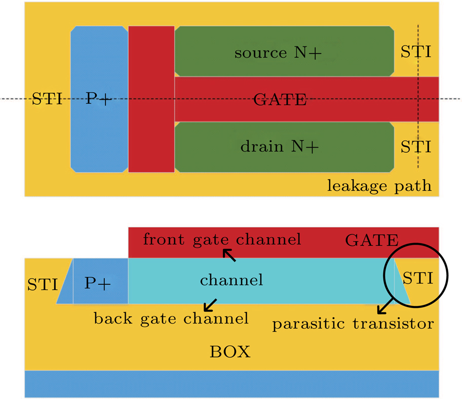
All the devices used in our experiments were fabricated in 0.13- SOI CMOS process. Processing was performed on a 200-mm diameter UNIBOND wafer from SOITEC. The top Si film was 100-nm and the buried oxide was 145 nm. As shown in Fig. 1, T-shape gate is introduced as the body contact. The STI connects with the buried oxide at the bottom for isolation. The device gate oxide thickness is about 1.8 nm. Different device sizes (W/L = 10/10, 0.15/10, 10/0.13, 0.5/0.13, and 0.15/0.13 in units of were chosen as samples in our study. All the samples were packed in Dual-In-Line ceramic packages. The operating voltage VDD is 1.2 V. The experiments were conducted in Xinjiang Technical Institute of Physics and Chemistry, the Chinese Academy of Sciences, and 60Co γ-ray was used as a radiation source. The dose rate was typically around 200 rad (Si)/s. During radiation exposure, the worst condition of ON bias for the STI was applied ( , ). The IV characteristics were measured by using a Keithley 4200 parameter analyzer before irradiation and after every step irradiation up to 100, 300, 500 krad (Si) for all devices. The transfer characteristics were measured under two constant drain biases ( or 1.1 VDD) for all devices at room temperature. The times of measurements were limited to half an hour after exposure to avoid annealing.

Fig. 1. (color online) (a) Top-view schematic and (b) cross section of T-shape layout of PD SOI nMOSFET with external body contact.
3. Results and discussion
3.1. Total ionizing dose effects in nMOSFETs

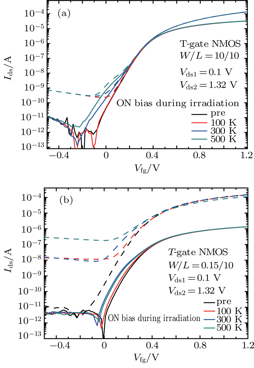
Figure 2(a) shows the front gate transfer characteristic curves of T-gate NMOS with W/L = 10/10 before and after ON bias radiation. There is no change in subthreshold region where the gate voltage is less than threshold voltage at 100 krad (Si) no matter what the high drain bias and low drain bias are. A little radiation-induced leakage current ( ) at and a significant subthreshold hump which are known as “STI corner leakage”[14] are observed for doses up to 300 krad (Si). When dose increases up to 500 krad (Si), the subthreshold hump becomes more serious. Figure 2(b) shows the front gate transfer characteristic curves of T-gate NMOS with W/L = 0.15/10 before and after ON bias radiation. For the low drain bias case, no obvious radiation-induced leakage current but a little threshold shift can be observed as doses rise up to 100 krad (Si). The threshold voltage negatively shifts with dose increasing gradually. For the high drain bias case, the radiation-induced leakage current appears and increases with the total dose going up. It is worthwhile to note that the subthreshold hump of the narrow device is more serious than that of the wide one. Because not only the STI parasitic transistor but also the main one in the narrow device suffers the influence of radiation-induced positive charges trapped in the STI oxide, which will be discussed later. Neither the wide nor narrow devices exhibit a significant radiation-induced off-state leakage current at low drain bias. This is different from the results of previous studies[1113] in PDSOI I/O NMOS where radiation-induced off-state leakage current can be observed obviously at the same TID level even in the case of a lower dose due to a lower body doping.

Fig. 2. (color online) Front gate curves of T-gate NMOS in logarithmic scale for the different-width transistors measured at low and high drain voltages ( and 1.32 V) before and after ON bias irradiation, at (a) and (b). Solid line represents low drain bias, dashed line denotes high drain bias.

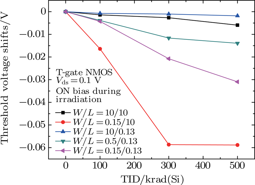
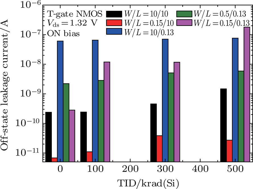
The threshold voltage of front-gate transistor is extracted by using the constant current method,[15] and it is defined as a critical gate voltage where the drain current reaches . Figure 3 shows the threshold voltage shifts of front gate transistors versus the total ionizing dose for PDSOI nMOSFETs with different channel sizes. It is interesting that the long channel device (W/L=10/10) shows a larger threshold voltage shift than the short one (W/L=10/0.13). This phenomenon is reported in Refs. [1618], indicating that the body doping concentration increases with channel length scaling down due to the fact that the halo or pocket implants result in non-uniform channel doping profiles along the device length. Hence, the of device with W/L = 0.15/10 is also larger than the one with W/L = 0.15/0.13. In terms of channel width, from Fig. 3, we can notice that the channel width is a key parameter for radiation degradation and that narrow channel devices show larger threshold voltage shifts. figure 4 shows the off-state leakage current variations versus the TID for different width-length-ratios after ON bias radiation. This figure shows the evidence that the narrow device is more sensitive to the TID than others, in which the radiation-induced leakage currents of the narrow and short device (W/L = 0.15/0.13) increase about three orders of magnitude after 500 krad (Si). In this paper, we focus on the influence of device width on the TID response.

Fig. 3. (color online) Threshold voltage shifts of front gate transistors versus the TID for PDSOI nMOSFETs with different channel sizes.
Fig. 4. (color online) Off-state leakage currents of PDSOI nMOSFETs with different channel sizes versus TID. Off-state leakage corresponds to drain current at .
3.2. TCAD device simulation analyses

As stated above, both the buried oxide and the STI oxide can potentially affect the TID responses of SOI transistors. To distinguish the degradations between the BOX-related case and the STI-related case after radiation, 3D TCAD device simulations are performed using Sentaurus’s Sprocess and Sdevice. The process parameters are provided by the foundry. The simulation models used include conventional drift-diffusion model, the bandgap narrowing model for carrier transport; the Shockley–Read–Hall model, band-to-band tunneling model, and avalanche generation model for generation-recombination; doping-dependent mobility degradation, high-field saturation, degradation at interfaces for mobility. Assume that the uniform effective sheet charge density is placed along the STI sidewall and the top silicon/BOX interface for post-radiation simulation, meanwhile ignoring any possible interface trap generation.

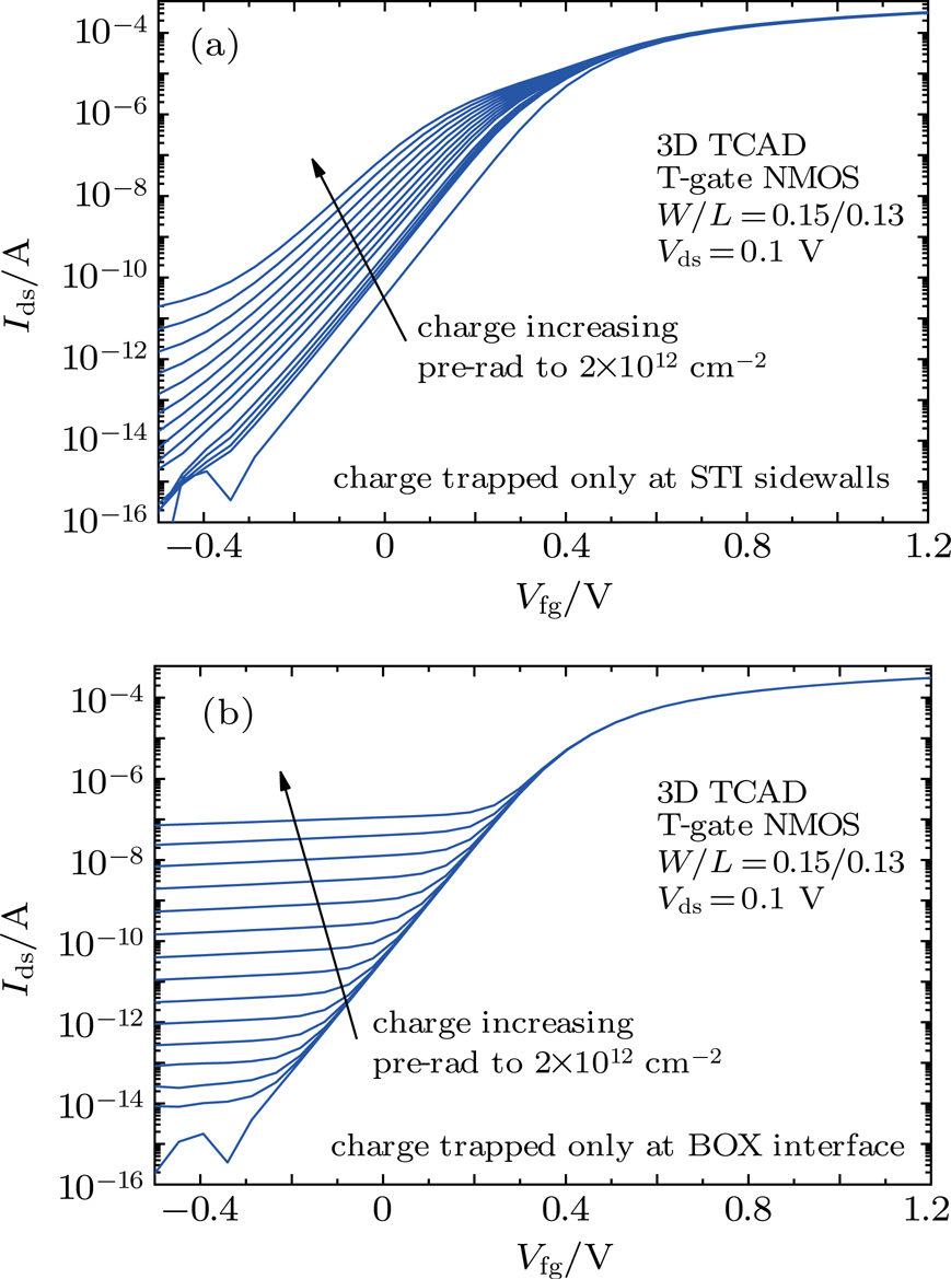
Figure 5 shows the simulated IV curves of device with W/L = 0.15/0.13 when sheet charges are just placed at the STI/silicon interface (Fig. 5(a)) and only placed at the silicon/BOX interface (Fig. 5(b)). For the STI charge case, a subthreshold hump as the true shift is observed and gradually gets strengthened with fixed charge density increasing. However, the BOX charge just causes the leakage to increase. In other words, the build-up of positive oxide trapped charges at the silicon/STI interface after TID radiation reduces the threshold voltage of the parasitic lateral transistor while the radiation-induced leakage current is related to both the STI case and the BOX case. In practice, the radiation-induced positive charge density and location mostly depend on the bias configuration during irradiation. In our experiment, ON bias configuration is chosen as the irradiation condition which is the worst bias for the STI reported in previous papers.[12,18,19] In that case, the electrical-field lines originating from the gate directly reach the silicon/STI interface where most of the radiation-induced positive charges are trapped. Thus the potential in the silicon is sufficiently modified to embody the negative threshold voltage shift . Hence, we will pay attention to the case of STI trapped charges to discuss the negative threshold voltage shift in the next section.

Fig. 5. (color online) Simulated pre-radiation, charge trapped (a) only at the silicon/STI interface and (b) only at the silicon/BOX interface for W/L = 0.15/0.13.

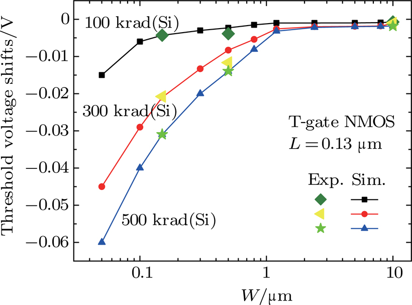
An additional insight into the TID sensitivities of such transistors related to their geometries, of simulated transistors induced by the positive charges trapped at the silicon/STI interface is extracted. Figure 6 shows the plots of transistor width W at various levels of positive charge densities (corresponding to total doses), in which the simulated results have good agreement with the experimental data. This figure exhibits a clear trend that the smaller the channel width, the higher the sensitivity to the TID is.

Fig. 6. (color online) Plots of simulated threshold voltage shift of T-gate NMOS transistor versus transistors width. Experimental data are shown by the larger symbols.
3.3. Enhanced radiation-induced narrow channel effects (RINCE)

The influence of channel width on TID response has been reported in bulk technology.[610] Most of the positive charges emerging during irradiation, which have escaped from the initial recombination, may be quickly trapped in the STI oxide along the conduction channel. The accumulation of positive charge eventually builds up a sufficient electric field to turn on an inversion channel where source–drain leakage current flows. For the narrow device, the accumulated positive charges at the STI edge not only determine the accumulation, depletion or inversion condition of the STI parasitic transistor (shown in Fig. 1(b)), but also has an influence on the electric field of the front main transistor. This reduces the source-to-drain and body-to-drain potential barriers, furthermore the threshold voltage, which is called radiation-induced narrow channel effect (RINCE).

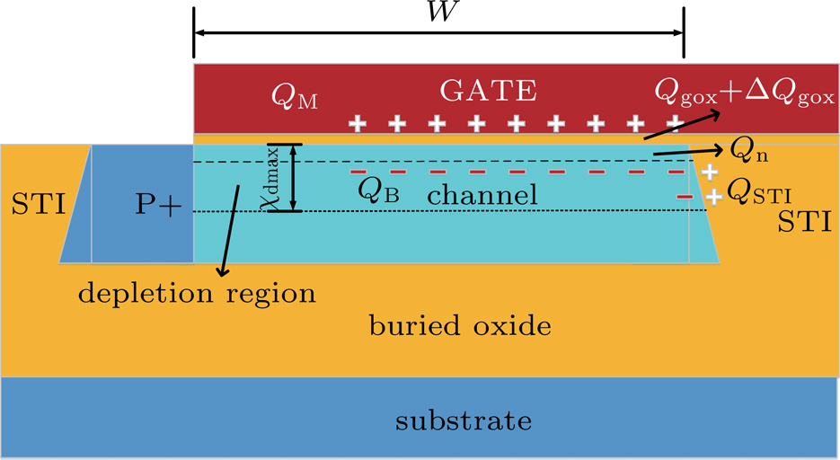
The RINCE for PDSOI NMOS can be explained by the charge sharing model as shown in Fig. 7. Following the charge conservation principle, the total charge quantity in the regions of the gate, the channel, the gate oxide, STI oxide can be rewritten as

where is the total charge quantity due to irradiation in the STI oxide below the depletion region, which is just balanced by its own mirror charge; is the total charge in the poly gate; is the general equivalent charge in the gate oxide before radiation, which includes the oxide trapped charge and interface states; is the increment of effective charge in the gate oxide due to irradiation; is the total charge in the inversion region; is the total impurity ionization charge in the depletion region. For the PDSOI devices, the silicon film thickness is larger than twice the maximum depletion width . In such a case, there is no interaction between the front and back depletion zones due to a neutral region beneath the front depletion zone. Hence, the threshold voltage model of PDSOI technology is similar to the bulk model,[20] the threshold voltage of NMOS in this work before irradiation can be described as
where is the work-function difference between the poly gate and the silicon, is the surface potential at the threshold point of inversion layer formation, is the front gate oxide capacitance per unit area, is the front gate area, and are reasonable to be assumed as zero before irradiation.

Fig. 7. (color online) The schematic illustration of the charge sharing model.

The positive charges induced by irradiation are trapped in the gate oxide ( and the STI oxide ( . The increment can result in the well-known threshold voltage shift of the main transistor, while the can cause two effects. One is to turn on the parasitic transistor through which STI sidewall leakage currents flow, and the other is the threshold voltage shift of the main transistor.[6] Notice that charges balances before irradiation, and can also balance a part of after irradiation, furthermore the quantity of charge balancing the total depletion charge is reduced, which is required in operation. After irradiation, equation (2) can be modified as

Comparing Eq. (2) and Eq. (3), the shift of front gate threshold voltage after irradiation is given by
As described above, the device gate oxide thickness is about 1.8 nm and the highest dose is only 500 krad (Si), can be ignored because less charges are trapped in the thin oxide (far less than 5 nm in thickness) in this work. Assume that a constant sheet charge density (in units of cm−2) trapped in the trench oxide which includes the effective oxide charge and the interface charge along the entire STI lateral walls. Only the charge above the maximum depletion width is useful in balancing the as figure 7 shows. Consequently, one can obtain
The proportion of the charge controlled by the STI is
then
From Eq. (7), it is clear that the front gate threshold voltage shift is inversely proportional to the channel width of main transistor. For the wide device, the charge quantity controlled by the STI is small compared with that controlled by the poly gate, and the is negligible. However, the proportion of the charge controlled by the STI rises drastically for the narrow device as shown in Eq. (6), so the shift of threshold voltage is remarkable.

3.4. Enhanced drain-induced barrier lowering (DIBL) effect versus channel width

The DIBL effect on the drain current of a short channel is well known. High drain-voltage-induced barrier lowering between source and channel causes reinforced electron injection, leading to the leakage current increasing. Radiation-enhanced DIBL effect was firstly observed by Youk et al.[21] Many papers have been published for total dose radiation-enhanced DIBL effect which focused on the influence of short channel and irradiation bias conditions. With the channel width decreasing, radiation-induced charges trapped in the STI oxide will lead to RINCE, which further increases the off-state leakage current affecting the DIBL effect. Now, we investigate the influence of channel width on DIBL effect under total ionizing dose effect. The DIBL effect parameter is defined as

In our experiment, is chosen to be 0.1 V, 1.1 VDD where . The DIBL parameter shift after irradiation can be expressed as
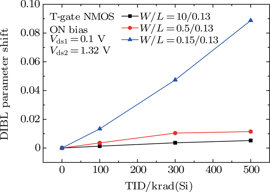
Figure 8 shows the plots of DIBL parameter shift versus total dose for different transistor sizes under ON bias irradiation. The DIBL parameter hardly shifts for the device with W/L = 10/0.13 after irradiation. For the device with W/L = 0.5/0.13, the DIBL parameter increases a little with the total dose increasing. However, the DIBL parameter increases sharply with W/L = 0.15 increasing to 0.13. These results indicate that the σ has a certain relationship with the channel width.

Fig. 8. (color online) DIBL parameter shifts versus total dose for different transistor sizes under ON bias irradiation.

This phenomenon may be explained by the following mechanisms. Radiation-induced positive charges trapped in the STI oxide and the buried oxide can both enhance the potential of the body, and the potential has a more significant change with high drain bias for the short channel device after irradiation. Then the lowering potential barrier at source causes the source injection to be enhanced, thus the enhanced DIBL effect is observed. However, the DIBL parameter for W/L = 10/0.13 device barely shifts. This indicates that the radiation-induced positive charges trapped in the buried oxide have almost no influence on the body potential. With the channel width narrowing, the influence of radiation-induced positive charges trapped in the STI oxide on the body potential become more obvious. Thus the radiation-enhanced body potential for the narrow device lowers the potential barrier at source, which furthermore causes the source injection to be enhanced. As a result, the enhanced DIBL effect occurs, which further degrades the device characteristics, such as the threshold voltage shift, the off-state leakage current increasing, the voltage gain decreasing, etc. Designers should take narrow devices into consideration when designing radiation-toleration ASICs.

4. Conclusions

An enhanced radiation-induced narrow channel effect (RINCE) in 0.13- PD SOI nMOSFETs is investigated in detail. The transformation from narrow channel effect (NCE) to reverse narrow channel effect (RNCE) is observed after irradiation. The charge sharing model can perfectly explain the experimental phenomena that the negative threshold voltage shift is inversely proportional to the channel width. The 3D TCAD simulations by placing sheet charge only at the STI lateral wall or the BOX interface distinguish between the relative influences of the STI and BOX charge components on the TID response. Radiation-induced charges trapped in the trench oxide can couple to the front gate channel and result in the threshold voltage shift. Furthermore, the enhanced DIBL effect occurs in the narrow device due to the fact that the STI trapped charges raise the surrounding body potential. These results would help IC designers to adjust mitigation strategies for radiation hardening. For the narrow SOI devices, edgeless geometry may be a good option.

Reference
[1] Auberton-Herve A J 1996 International Electron Devices Meeting, December 8–11, 1996 San Francisco, CA, USA 3
[2] Schwank J R 1997 Microelectron. Eng. 36 335342
[3] Barnaby H J 2006 IEEE Trans. Nucl. Sci. 53 3103
[4] Snoeys W et al. 2000 Nucl. Instrum. Method Phys. Res. 439 349
[5] Saks N S Ancona M G Modolo J A 1984 IEEE Trans. Nucl. Sci. 31 1249
[6] Faccio F Cervelli G 2005 IEEE Trans. Nucl. Sci. 52 2413
[7] Chen J Y Henderson R C Martin R Patterson D O 1982 IEEE Trans. Nucl. Sci. 29 1681
[8] Gaillardin M Goiffon V Girard S Martinez M Magnan P Paillet P 2011 IEEE Trans. Nucl. Sci. 58 2807
[9] Faccio F Michelis S Cornale D Paccagnella A Gerardin S 2015 IEEE Trans. Nucl. Sci. 62 2933
[10] Bezhenova V Michalowska-Forsyth V 2016 Asia-Pacific International Symposium on Electromagnetic Compatibility May 17–21, 2016 Shenzhen, China 366
[11] Huang H X Bi D W Peng C Zhang Y W Zhang Z X 2013 Chin. Phys. Lett. 30 080701
[12] Peng C Hu Z Zhang Z Huang H Ning B Bi D 2014 Nucl. Instrum. Method Phys. Res. 748 7078
[13] Ning B Bi D Huang H Zhang Z Chen M Zou S 2013 Microelectron. J. 44 8693
[14] Turowski M Raman A Schrimpf R D 2004 IEEE Trans. Nucl. Sci. 51 3166
[15] Ortiz-Conde A García Sánchez F J Liou J J Cerdeira A Estrada M Yue Y 2002 Microelectron. Reliab. 42 583
[16] Alles M L Hughes H L Ball D R McMarr P J Schrimpf R D 2014 IEEE Trans. Nucl. Sci. 61 2945
[17] Zhang M Y Hu Z Y Zhang Z X Fan S Dai L H Liu X N Song L 2017 Chin. Phys. Lett. 34 088501
[18] Ning B Bi D Huang H Zhang Z Hu Z Chen M Zou S 2013 Microelectron. Reliab. 53 259
[19] Fan S Ning B Hu Z Zhang Z Bi D Peng C Song L Dai L 2016 Microelectron. Reliab. 56 19
[20] Neamen D A 2011 Semiconductor physics and devices: basic principles 4 New York McGraw-Hill 385 390
[21] Youk G U Khare P S Schrimpf R D Massengill L W Galloway K F 1999 IEEE Trans. Nucl. Sci. 46 1830