Growth and characterization of AlN epilayers using pulsed metal organic chemical vapor deposition
Ji Zesheng1, Wang Lianshan1, 2, †, Zhao Guijuan1, Meng Yulin1, Li Fangzheng1, Li Huijie1, Yang Shaoyan1, Wang Zhanguo1
Key Laboratory of Semiconductor Materials Science, Institute of Semiconductors, Chinese Academy of Sciences, Beijing 100083, China
College of Materials Science and Opto-Electronic Technology, University of Chinese Academy of Sciences, Beijing 100049, China


† Corresponding author. E-mail: ls-wang@semi.ac.cn

Abstract

We report the growth of AlN epilayers on c-plane sapphire substrates by pulsed metal organic chemical vapor deposition (MOCVD). The sources of trimethylaluminium (TMAl) and ammonia were pulse introduced into the reactor to avoid the occurrence of the parasitic reaction. Through adjusting the duty cycle ratio of TMAl to ammonia from 0.8 to 3.0, the growth rate of AlN epilayers could be controlled in the range of 0.24 m/h to 0.93 m/h. The high-resolution x-ray diffraction (HRXRD) measurement showed that the full width at half maximum (FWHM) of the (0002) and (10-12) reflections for a sample would be 194 arcsec and 421 arcsec, respectively. The step-flow growth mode was observed in the sample with the atomic level flat surface steps, in which a root-mean-square (RMS) roughness was lower to 0.2 nm as tested by atomic force microscope (AFM). The growth process of AlN epilayers was discussed in terms of crystalline quality, surface morphology, and residual stress.

1. Introduction

AlN and AlGaN based materials have potential applications in power electronic and optoelectronic fields due to their wide energy bandgaps, high electron mobilities, high breakdown voltages, and strong resistance to radiation.[1] For optoelectronic devices, an AlN layer can be usually used as a template layer or window layer for light-emitting and photo-detective devices in the ultra-visible (UV) spectral region from 200 nm to 365 nm. These UV devices can be used in areas such as disinfection/sterilization, homeland security, and secure space-to-space communication.[2,3] For application in power electronic devices such as the field effect transistor (FET) and high electronic mobility transistor (HEMT), an AlN layer can be used both as a spacer layer, which significantly influences the electron mobility in the two-dimensional electron gases, and a buffer layer when the devices are grown on semi-insulating SiC or Si substrates.[4] However, growing high quality AlN films on foreign substrates using a routine metal organic chemical vapor deposition (MOCVD) method at low temperature ()[5] remains a challenge due to the cracking arising from the large lattice mismatch and difference of thermal expansion coefficients between the epilayer and the substrate, severe gas-phase parasitic reactions between trimethylaluminium (TMAl) and ammonia, and poor migration ability of Al atoms on the AlN surface.[6] Many researchers have proposed different models or explanations[712] for the growth kinetics of AlN, but by only taking into account some factors like parasitic reactions, grain boundaries, and dislocations. These models are still hard to precisely predict the AlN growth process and determine the cause of poor AlN quality.

In this study, we grow good quality AlN epilayers on sapphire by a pulsed MOCVD method at a relative low temperature (1150 °C–1190 °C) and find three kinds of growth modes (step-flowing mode, step-bunching mode, and island growth mode) depending on the process parameters. The crystalline quality, surface morphology, and residual stress are characterized and the growth kinetics is discussed. The realization of AlN epilayers with good crystalline quality would be beneficial to the development of the UV optoelectronic and power electronic devices.

2. Experiment

AlN samples were grown on 2-inch c-plane sapphire substrates in a low-pressure AIX 200/4 RS-F MOCVD reactor. Trimethylaluminium (TMAl) and ammonia (NH3) were used as Al and N sources, respectively. Prior to growth, the sapphire surface was thermally cleaned in hydrogen ambient for 10 min, followed by AlN growth in a pressure of 50 mbar. To avoid the gas parasitic reactions of TMAl and NH3, TMAl and NH3 were pulse introduced into the reactor by a pulsed MOCVD method. Here we used the duty cycle ratio of TMAl to NHβ, to define the growth atmosphere of AlN for the chamber pressure and the carrier gas flow was constantly maintained for all the samples. The value of β changed from 0.8 to 3.0 so that the growth rate of the AlN epilayers could be controlled, as schematically shown in Fig. 1. Such a growth process was in-situ monitored by Filmetrics F30. When either the TMAl flow or NH3 flow was switched off, the hydrogen flow was swept to purge the source residual gas. The growth pressure was maintained at 50 mbar during the whole growth process. The temperatures for the nucleation (), the growth temperature for the subsequently-grown coalescence and continuous film () are presented and other source flow rates are also given in Table 1.

Fig. 1. (color online) Diagrams of pulse growth mode of AlN samples.
Table 1.

Growth parameters of AlN samples.

.

The crystalline quality of AlN epilayers was examined by a high resolution x-ray diffractometer (HRXRD) installed at a diffuse x-ray scattering station of the Beijing Synchrotron Radiation Facility, and a Huber five-circle diffractometer was used. The radiation energy of the x-ray beam was 8.05 keV with 0.7 mm×0.4 mm () of the spot size. The surface morphology and surface roughness were characterized using an atomic force microscope (AFM) in tapping mode. The stress in AlN was determined through the Raman shift of characteristic AlN- peaks, measured by a LabRAM HR 800 Raman spectrometer with a 514.5 nm-line laser as the excitation source.

3. Results and discussion

Under high temperature conditions and free of the parasitic reaction, AlN growth rate G is mass transport limited, which means that the growth rate should be proportional to the TMAl flow rate. However, due to the strong parasitic reaction of TMAl and ammonia, the growth rate is very sensitive to the growth atmosphere like the V/III ratio. The possible reaction pathways are described in Fig. 2. When TMAl and ammonia flow above the heated substrate, they begin to merge and form the main product DMAlNH2 (Al(CH3)2:NH2) through adduct reactions.[13] DMAlNH2 tends to form dimer ([DMAlNH2]2), trimer ([DMAlNH2]3), and complex [DMAlNH2]n compounds. The thermophoretic force makes the trimer float over the dimer, the dimer is therefore the main precursor for AlN epilayers while the trimer is for AlN particles.

Fig. 2. Schematic of the AlN deposition and reaction pathways.[13]

The reflectance versus time curves of AlN growth in-situ optically monitored by Filmetrics F30 with selective wavelength at 650 nm are shown in Fig. 3. The boundary for the AlN nucleation and coalescence growths is marked by the arrows. The layer thickness and growth rate[14] of the AlN layer can be calculated by

where λ is the wavelength, n is the reflective index, d is the layer thickness, and i is an integer which corresponds to the oscillation periods. The growth rate G derived by the above-mentioned equation is summarized in Table 2.

Fig. 3. (color online) Reflectance versus time of AlN samples measured at 650 nm.
Table 2.

Growth rate G and the other correlative parameters.

.

The diffusion coefficient D and the rate of adsorption and desorption of Al atoms follow the Arrhenius equation

where D0 is the maximal diffusion coefficient (at infinite temperature), k is the rate constant, T is the absolute temperature, A is the pre-exponential factor, is the activation energy for the reaction, and R is the universal gas constant.

To determine the extent of the reaction of TMAl, the relative efficiency value γ is introduced as

where G is the growth rate of AlN, is the actual TMAl flow participating in the growth, which is the ratio of the flow of TMAl introduced to the reactor to the on-duty time. B is the normalization constant and here we take B = 60 to make γ more comparable. In terms of the physical meaning, the larger the value of γ is, the stronger the reaction of TMAl is. The calculated values of γ are shown in Table 2.

To confirm the validity and examine the quantitative relationships of β with , G, and γ, we introduce two additional similar AlN samples which are labeled as E and F, and the corresponding parameters are listed in Table 2.

Three key factors, the actual TMAl flow, growth temperature T, and growth atmosphere, that may influence the growth rate of AlN are considered. It can be easily concluded that the value of has little impact on the growth rate of AlN as seen from Table 2, thus we assume that has reached the saturation value.[13] The temperature ranged from 1150 °C to 1190 °C in the experiments, such small temperature fluctuation has little influence on the diffusion coefficient and the rate of adsorption and desorption according to Eqs. (2) and (3). Therefore, the influence of the fluctuation of and temperature can both be neglected. After excluding the first two factors, we assume that the growth atmosphere is the primary factor that determines the growth rate of AlN.

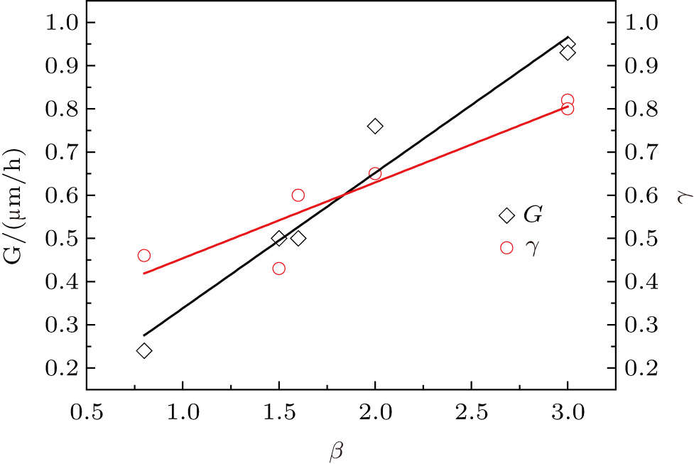
A linear fitting of β with growth rate G and relative efficiency value γ is performed and the results are shown in Fig. 4. The fitting factors R2 are 0.96 and 0.85, respectively, which means a good linearity. This indicates that larger β can induce a higher extent of reaction of TMAl and a higher growth rate of AlN. To put it in another way, when β increases, the formed [DMAlNH2]n species turn to a dimer form as shown in Fig. 2, thus the extent of the reaction of TMAl and the growth rate of AlN are both improved.

Fig. 4. (color online) The linear fitting of β with G and γ.

To explain the nature of the approximate proportional relationship of β with growth rate G and the relative efficiency value γ, we speculate that it can be attributed to the change of the growth atmosphere, i.e., the ammonia flow is switched to hydrogen flow corresponding to the transition from the N-rich condition to the H-rich condition. Gherasoiu et al.[15] pointed out that the AlN growth rate is limited by the degree of hydrogen passivation and the nitrogen bonds available at the growth surface. Under the N-rich condition (when the ammonia flow is switched on), the hydrogen surface coverage increases, which means that Al has to compete with residual hydrogen for N bonds, thus resulting in a reduced growth rate. To conclude, it is a feasible method to modify the growth rate of AlN growth by adjusting the duty cycle ratio of TMAl to ammonia when the TMAl flow has reached the saturation point.

The nucleation layer in sample A was directly grown on the sapphire substrate at 1150 °C, while the other samples were grown at 800 °C. As shown in Fig. 3, oscillations in the intensity of sample A do not show an obvious drop, and have a similar tendency to those of the other samples in the growth process. However, the macro surface morphology of sample A is less uniform with some opaque areas on the 2-inch size wafer, while the other three samples show featureless specular surfaces. According to Ching’s study,[16] the sapphire substrate may have undergone an unintentional nitridation process at the initial growth stage of high temperature (above 950 °C) AlN nucleation layer, therefore giving rise to the mixed polarity and rough surface. In light of Ching’s study and our results, a lower nucleation temperature can improve the uniformity and morphology of the AlN layer. The following measurements were all conducted in the transparent featureless areas of these AlN layers.

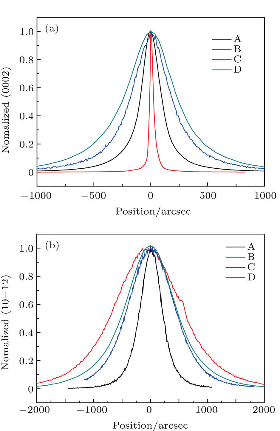
Symmetrical (0002) and asymmetrical (10-12) x-ray rocking curve measurements (XRC) were carried out to evaluate the crystalline quality of the AlN samples as shown in Fig. 5. The full widths at half maximum (FWHMs) for sample A from (0002) and (10-12) reflections are 194 arcsec and 421 arcsec, respectively. The corresponding FWHMs can reflect the densities of screw-type dislocations and edge-type dislocations respectively.[17] The density of ρ dislocations can be calculated through the following equation by Hirsch mode:[18]

where δ is the FWHM, and is the burgers vector of dislocation. In the case of AlN, the values of the burgers vectors are 0.498 nm for the screw dislocation and 0.3112 nm for the edge dislocation. The densities of the screw dislocations (screw DT) and the edge dislocations (edge DT) are shown in Table 3 for the four samples. The edge dislocation density in sample A is lower than that in the other samples, and the screw dislocation density is also relatively lower than that in samples C and D, but slightly higher than that in sample B. The reason is not clear currently and a further study is underway.

Fig. 5. (color online) X-ray rocking curves of AlN (0002) and (10-12) reflections measured by HRXRD.
Table 3.

XRD, AFM, and Raman measurement results of AlN samples.

.

Raman scattering measurements were performed to evaluate the residual stress in the AlN layer[19] as shown in Fig. 6. Only the E2 (high) mode can be observed for all samples in the configuration. The results are presented in Table 3. It has been reported that the peak of bulk AlN under zero stress is about 657.4 cm−1. Samples A and B are fully relaxed, while samples C and D have residual tensile strains[20,21] of 0.55±0.05 GPa and 0.18±0.02 GPa, respectively.

Fig. 6. (color online) Raman spectra of the AlN samples.

Figure 7 shows the atomic force microscopic images for the four samples. In sample A, an atomic level flat surface feature can be seen with an RMS roughness of 0.2 nm and a terrace width of ∼100 nm, implying single monolayer height steps. Bryan et al.[22] reported that the critical terrace width of AlN in step-flow mode is about 60–110 nm, in agreement with our result. In addition, there are some kinks on the surface, this can be ascribed to the impact of the dislocations.[23] The step-flow growth mode contributes to the high quality AlN films. The large islands with different sizes in sample B indicate the low island density and the island growth mode. Due to the large distance between the islands, the coalescence and flatness of the AlN are poor and this is in agreement with the RMS roughness of 20.7 nm. Moreover, the coalescence of islands could cause the tilt of the islands and thus degrades the crystalline quality. As shown in Fig. 1, in the growth cycle of sample B, the TMAl off-duty time is 5 s, e.g., the TMAl flow stopped flowing to the reactor, but the ammonia flow started on, which equals an infinite V/III ratio. Wang et al.[24] found that a high V/III ratio leads to a high longitudinal growth rate, forming island crystals to produce abundant crystal boundaries that are capable of suppressing the elongation of dislocation, which is in agreement with the especially low FWHM of 36 for the (0002) reflection.

Fig. 7. (color online) AFM micrographs of AlN layers of (a) sample A, (b) sample B, (c) sample C and (d) sample D.

In sample C, there is a step-bunched morphology with 5–10 ML-height steps and width terrace. According to the Raman spectra, sample C has residual tensile strain. Tersoff et al.[25] reported that elastic relaxation at steps produces a long-range attractive interaction between the steps and thus the surface is unstable against step-bunching. Suda et al.[7] reported the transition from step-bunching to step-flow mode for AlN growth on SiC substrate. The step-bunching mode and the transition to step-flow mode were both observed as shown in Fig. 8, and it agrees with the above-mentioned reports. Compared with sample A, sample C has an inferior crystalline quality whose FWHMs for (0002) and (10-12) reflections are almost doubled and the reaction efficiency value γ decreases from 0.6 to 0.43. This means that the strain or the step-bunched morphology may inhibit the adsorption of Al adatoms and thus decrease the efficiency value γ as well as degrade the crystalline quality. Sample D did not present a remarkable growth mode just by judging from the AFM image shown in Fig. 6. It should be noted that sample C and sample D have similar crystalline quality and RMS values but a significant difference in the surface morphology. These two samples had exactly the same growth conditions except the value of β, which can be reflected in the growth rate G. Therefore, we assume that the change of the growth rate has an impact on the surface morphology. One possible explanation is that the higher growth rate of sample D suppressed the step-bunching mode[25] that should present in sample C, furthermore, the residual strain was partially relaxed as shown in Table 3.

Fig. 8. (color online) The height distributions of (a) line 2 and (b) line 1 from the AFM micrograph of sample C.
4. Conclusion

We studied the growth of AlN layers using pulse MOCVD methods and obtained a high quality AlN layer under a relative low temperature. The growth rate of AlN was adjusted by the on-duty time ratio of TMAl flow to ammonia. We found that a low temperature nucleation layer (about 800 °C) can improve the uniformity of the AlN layer while there is a narrow growth window to grow a high quality AlN film with a high temperature nucleation layer (about 1150 °C). Three different growth modes were observed in our samples including step-flow mode, step-bunching mode, and island growth mode.

Reference
[1] Collazo R Mita S Xie J Rice A Tweedie J Dalmau R Sitar Z 2011 Phys. Status Solidi 8 2031
[2] Xie J Mita S Bryan Z Guo W Hussey L Moody B Schlesser R Kirste R Gerhold M Collazo R 2013 Appl. Phys. Lett. 102 171102
[3] Taniyasu Y Kasu M Makimoto T 2006 Nature 441 325
[4] Ren C Zhong S Li Y Li Z Kong Y Chen T 2016 Journal of Semiconductors 37 084002
[5] Sun X Li D Chen Y Song H Jiang H Li Z Miao G Zhang Z 2013 Crystengcomm 15 6066
[6] Creighton J R Wang G T Breiland W G Coltrin M E 2004 J. Cryst. Growth 261 204
[7] Suda J Noriojima A Kimoto T Matsunami H 2003 MRS Online Proceeding Library 798
[8] Daudin B Feuillet G Mula G Mariette H Rouviére J L Pelekanos N 1999 Phys. Status Solidi 176 621
[9] Dauelsberg M Brien D Rauf H Reiher F Baumgartl J Hberlen O Segal A S Lobanova A V Yakovlev E V Talalaev R A 2014 J. Cryst. Growth 393 103
[10] Hsu K Y Chung H C Liu C P Tu L W 2007 Appl. Phys. Lett. 90 211902
[11] Sun X Li D Chen Y Song H Jiang H Li Z Miao G Zhang Z 2013 CrystEngComm 15 6066
[12] Takano K Saito Y Pierre-Louis O 2010 Phys. Rev. 82 2195
[13] Mihopoulos T G Gupta V Jensen K F 1998 J. Cryst. Growth 195 733
[14] Breiland W G Killeen K P 1995 J. Appl. Phys. 78 6726
[15] Gherasoiu I Nikishin S Kipshidze G Borisov B Chadolu A Ramkumar C Holtz M Temkin H 2004 J. Appl. Phys. 96 6272
[16] Huang W C Chu C M Wong Y Y Chen K W Lin Y K Wu C H Lee W I Chang E Y 2016 Mater. Sci. Semicond Process 45 1
[17] Heinke H Kirchner V Einfeldt S Hommel D 2000 Appl. Phys. Lett. 77 2145
[18] Dumn C G Koch E F 1957 Acta Metall 5 548
[19] Davydov V Y Kitaev Y E Goncharuk I N Smirnov A N Graul J Semchinova O Uffmann D Smirnov M B Mirgorodsky A P Evarestov R A 1998 Phys. Rev. 58 12899
[20] Sarua A Kuball M Van J E 2002 Appl. Phys. Lett. 81 1426
[21] Trodahl H J Martin F Muralt P Setter N 2006 Appl. Phys. Lett. 89 3498
[22] Bryan I Bryan Z Mita S Rice A Tweedie J Collazo R Sitar Z 2016 J. Cryst. Growth 438 81
[23] Bryan I Bryan Z Mita S Rice A Hussey L Shelton C Tweedie J Maria J P Collazo R Sitar Z 2016 J. Cryst. Growth 451 65
[24] Wang T Y Liang J H Fu G W Wuu D S 2016 CrystEngComm 18 9152
[25] Tersoff J Phang Y H Zhang Z Lagally M G 1995 Phys. Rev. Lett. 75 2730