High quality factor superconducting coplanar waveguide fabricated with TiN
Liu Qiang1, Xue Guang-Ming2, Tan Xin-Sheng1, Yu Hai-Feng1, 3, †, Yu Yang1, 3,
National Laboratory of Solid State Microstructures, Nanjing University, Nanjing 210093, China
Key Laboratory of Quantum Information, University of Science and Technology of China, Hefei 230026, China
Synergetic Innovation Center of Quantum Information & Quantum Physics, University of Science and Technology of China, Hefei 230026, China


† Corresponding author. E-mail: hfyu@nju.edu.cn yuyang@nju.edu.cn

Abstract

We fabricated TiN coplanar waveguides using standard lithography techniques followed by ICP etch. In order to achieve high quality factor, we investigated the film growth by choosing different deposition conditions for various substrates. Quality factors of waveguide resonators were measured at 20 mK in both high and low microwave power limits. An inner quality factor of several million was achieved at high power limit for a predominantly (200)-oriented TiN film which was grown on HF cleaned silicon wafer. A quality factor of larger than one million was achieved at high power limit for TiN film grown on sapphire.

1. Introduction

The recent progresses on superconducting quantum computation suggest that superconducting quantum circuits are promising approaches to realize scalable quantum computation.[15] Currently, the most common circuitry design for manipulating and reading the superconducting qubits is a circuit QED system, which consists of a superconducting qubit coupled with coplanar waveguides (CPW) or 3D cavities.[69] The coplanar waveguides are crucial parts for qubit manipulation and measurement. In addition, the coplanar waveguides also serve as couplers to couple different qubits together.[1, 10] Therefore, the property of coplanar waveguide has a great influence on the performance of qubit.[11] It is found that high quality factor, which means low loss, is a preliminary for long resonant lifetimes and better resolved frequencies, leading to a longer qubit decoherence time and higher signal-to-noise ratio for qubit measurement.[12]

The essential issues that affect quality factor of CPW include the electric resistance, the quality of the film, the participation ratio,[13] and the substrate. Since superconducting materials below the critical temperature exhibit zero electric resistance, Al, Nb, and Re are widely used to fabricate high quality factor CPW in superconducting quantum circuits. The typical value of the quality factor of these CPW is about in the high power regime. When the power decreases to low power regime which corresponds to several photons level, their quality factor will decrease to about . The power dependence of the quality factor comes from the two-level systems (TLSs) which result from the unsaturated bonds in the interface between superconducting film and substrate as well as the exposed surfaces of CPW.[14, 15] The energy dissipated by TLSs are saturated at high power, while their effect increases significantly at low power, resulting in a decrease of quality factor.[16]

In order to further increase the quality factor of CPW, people have tried to minimize the TLSs in the materials. It is found that nitrides are very stable even against oxidation.[12] Superconducting coplanar waveguide based on nitrides has shown very high quality factor in high power regime. Recently, several groups have reported CPWs of high quality factors made of TiN and NbTiN, respectively.[17, 18] However, voltage bias and deep etching are used in these processes, increasing the unwanted variation of the fabrication. Moreover, the toxicity of HMDS the Delft group used to clean substrate makes the process more dangerous. Here, we simplify the procedures by using standard lithography techniques followed by ICP etch. We investigate the optimal deposition conditions for TiN film. An inner quality factor of several million is achieved at high power limit for a predominantly (200)-oriented TiN film which is grown on HF cleaned silicon wafer. A quality factor of larger than one million is achieved for TiN film grown on sapphire at high power limit. These figures of merit are comparable to those reported in previous processes.

2. Experiment

By using reactive DC sputtering system, we deposit TiN films onto both high resistivity (> 10 k cm) silicon (100) substrates and sapphire (0001) substrates. All substrates are prepared by rinsing sequentially in acetone, ethanol, and DI water in an ultrasonic bath to remove any contaminant. Part of silicon substrates are further cleaned in HF solution (1:10 HF:H O) to remove any native oxide and also to terminate the surface with hydrogen. Substrates are loaded into the sputter chamber immediately after cleaning in case of secondary pollution in ambient pressure. The base vacuum of the sputter chamber is about Pa. The argon and nitrogen gas and titanium target are all of ultra-high purity (> 99.99%). Different sputter parameters, i.e., with/without HF cleaning, nitrogen gas flow (8, 6, 4, 2, in units of sccm), total gas pressure (0.4, 0.6, 0.8, in unit of Pa), were tested to search a best condition for the growth of TiN film. Input flow of argon gas was fixed at 12 sccm. By using the deposition rate of about 4 nm/min, we deposit 30 nm thickness TiN film on silicon substrate and 50 nm thickness TiN film on sapphire substrate. We observe the crystallization direction by the spectrum of XRD. Surface flatness was scanned by atomic force microscope (AFM). RF coplanar waveguides were patterned by standard lithography technique followed by ICP SF etch. For the waveguides, the width of the center strip and gap are 10 μm and 6 μm, respectively. For the feed line the width of the center strip and gap are 15 μm and 9 μm, respectively. This center to gap width ratio is designed for matching a 50 Ω impedance. Sample chips are stuck to a copper sample box by GE vanish and wire-bonded to PCB board. The copper box is cooled to 20 mK in a dilution refrigerator (Oxford DR200). To protect the chip from the external noise, we add attenuators in the input line on several cold plates (−6 dB on PT1 plate, −10 dB on PT2 plate, −10 dB on Still plate, −20 dB on MC plate) of the DR. Two circulators were connected to the output port of the copper box to block back scattered signals. The output signal was amplified by an HEMT at the 4 K stage of the DR. Microwave transmission curve ( ) was measured by a network analyzer.

3. Results and discussion

The quality of the film is one of the important issues to the quality factor of CPW. At first, we investigate the influence of HF cleaning on the growth of TiN film. Two groups of TiN films are sputter-deposited onto silicon substrate with and without HF cleaning. The nitrogen gas flow was set at either 6 or 8 sccm while the argon gas flow was always 12 sccm. Total gas pressure is kept at 0.4 Pa and the substrates are preheated to 500 °C before deposition. XRD results of these TiN films are shown in Fig. 1. The sharp peaks around 33° come from silicon substrate. Peaks around 42.5° are the characteristic peak of (200)-TiN. No characteristic peak of (111)-TiN is present, which means all the films are grown with only (200)-TiN priority. It is found that HF cleaning will increase the (200) peak. This suggests that HF etching has a positive effect on the growth of (200)-TiN film on silicon substrate. In addition, SiN buffer has been reported to be important for the growth of (200)-TiN. However, the silicon substrate without HF cleaning is believed to have a native oxide layer on the surface instead of SiN buffer which would form on bare and pure silicon substrate during pre-deposition.[19] We have successfully deposited (200)-TiN film on silicon substrate without the presence of thin SiN buffer layer.

Fig. 1. (color online) XRD results of TiN films grown on silicon substrates with and without HF cleaning. Peaks around 42.5° are the characteristic peak of (200)-TiN. Sharp peaks around 33° come from the silicon substrate.

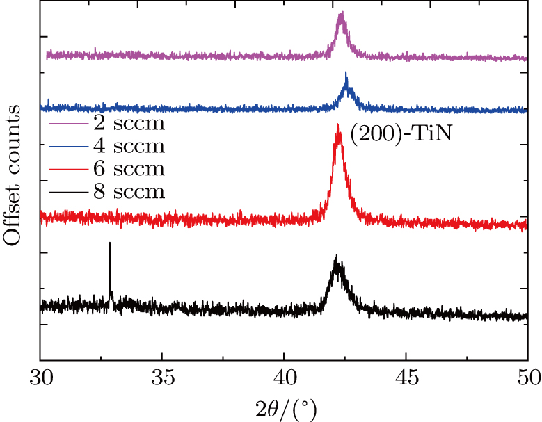
Since we used reactive DC sputter method, the nitrogen gas percentage may have an influence on the growth of TiN films. We change the nitrogen gas flow (2, 4, 6, 8 sccm) while keeping the argon gas flow at 12 sccm and total pressure at 0.4 Pa. All the silicon substrates are cleaned by HF solution before being loaded to sputter chamber and are heated to 500 °C before deposition. From the XRD results, we can know that all the four films exhibit (200)-TiN growth priority and no (111)-TiN characteristic peak can be seen. From the height and FWHM of the peaks, we can consider nitrogen gas flow of 6 sccm as an optimum condition for (200)-TiN to grow.

We also investigate the effect of the total pressure on the film. Shown in Fig. 3 is the XRD result of TiN films grown in different total gas pressure. Substrates are chosen as silicon wafers cleaned by HF solution. Nitrogen and argon gas flow are kept at 8 and 12 sccm respectively. The substrates are all preheated to 500 °C before deposition. We can see that the TiN film grown in the lowest pressure 0.4 Pa has a significant (200)-TiN peak, while the other two films only have vague peak shape.

Fig. 3. (color online) XRD result of TiN films grown in different total gas pressures.

Besides investigating the crystallization of TiN films, we also measure the flatness of the film surface. AFM scans of TiN films grown in different nitrogen gas flow are shown in Fig. 4. All the films are deposited at the same conditions as samples in Fig. 2. We can see that with the decreasing of nitrogen gas flow, the film is becoming much more flat. A flat surface may reduce the surface participation which would benefit the coherence time.[13]

Fig. 2. (color online) XRD results of TiN films grown with different nitrogen gas flow.
Fig. 4. (color online) AFM image of TiN films on silicon substrate.

To summarize the optimum TiN film growth condition, we find that HF cleaning has a positive effect on the growth of (200)-TiN film on silicon substrate. The high nitrogen to argon ratio limit might not be the best choice. A lower total pressure and medium nitrogen gas percentage can result in a good TiN film with only (200) orientation.

It is find that the quality factor of the CPW relies on the loss of the substrate. In order to decrease the loss of CPW, people have broadly used sapphire instead of silicon as substrates in superconducting quantum circuits.[20, 21] We use sapphire substrate for comparison. Similar to that of the silicon substrate, we sputter the TiN film on a sapphire at 500 °C, 0.4 Pa total pressure, 6 sccm nitrogen flow, and 12 sccm argon flow. The XRD spectrum of TiN film on sapphire is shown in Fig. 5. The peak around 37.5° is the characteristic peak of (111)-TiN, while the peak around 43° is of (200)-TiN. Different from the film on silicon substrate, TiN film on sapphire exhibits two crystallization directions.

Fig. 5. XRD result of TiN film grown on sapphire. (111)-TiN peak at 2θ around 37.5° and (200)-TiN peak at 2θ around 43° are both present.

Using standard lithography technique followed by ICP SF etch, we pattern CPWs on as-grown TiN films on silicon and sapphire substrates. CPWs are constituted by quarter-wavelength waveguides coupled to a common feed line. Microwave transmission curves are measured at 20 mK with network analyzer. Resonant peaks are fitted by the following formula:[18]

where A is the transmission away from the resonance. α allows a linear variation in the overall transmission chain in the narrow frequency range around any given resonance peak. is the resonance frequency. is the loaded quality factor of the resonator, which determines the inner quality factor with via . is a complex-valued quality factor related to via . The imaginary part of gives rise to an asymmetry in the resonance peak line shape.

A full transmission curve of waveguide resonators fabricated on TiN film which grown on silicon substrate is shown in Fig. 6(a). The growth conditions are 500 °C, 0.4 Pa total pressure, 6 sccm nitrogen flow, 12 sccm argon flow, and the silicon substrate was cleaned by HF solution. Figure 6(b) shows a curve fitting with R-square of 0.9998 of the resonant peak at 5.405 GHz (dashed box). From the fitting data, we obtain of 9.213 × , of 7.559 × , and α of −0.6405, which result in an inner of 4.05 × .

Fig. 6. (color online) (a) Full transmission curve of waveguide resonators fabricated on TiN film which grown on silicon substrate. (b) Zoomin of the resonant peak for the resonator located at 5.405 GHz (blue dashed box).

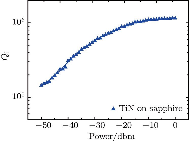
Usually, the quality factor of CPW depends on the input power. We measure the quality factor versus the input power of one TiN waveguide resonator in Fig. 7. The substrate is sapphire. We obtain quality factor of about 1.2 × in multi-photon limit and about 1.5 × in single-photon limit. Although, TiN film on sapphire exhibits a high quality factor enough for sustaining a long coherence lifetime for qubits. Compare TiN film grown on sapphire with that grown on silicon substrate, the later one can exhibit a higher quality factor. This agrees with the loss analysis that (200)-TiN has a lower rf loss than (111)-TiN.

Fig. 7. (color online) Inner quality factor (in logarithm to base 10) dependence on input power of CPW fabricated on TiN film grown on sapphire. The solid line represents a smooth curve of . Inner quality is about 1.2 × in multi-photon limit while it is about 1.5 × in single-photon limit.
4. Conclusion

In conclusion, we have investigated TiN films grown in different conditions, i.e., with/without HF cleaning, nitrogen to argon gas flow ratio, total pressure, silicon/sapphire substrate. XRD and AFM are utilized to characterize the crystallization and surface topography respectively. Generally, (200)-TiN has been successfully obtained on silicon substrate both with and without HF cleaning. They have shown a high quality factor at multi-photon level. TiN film on sapphire is a mixture of (111)-TiN and (200)-TiN. However, it still shows a low loss at both multi and single photon limit. These high quality factor CPWs are promising for sustaining a long coherence life time of quantum states.

Reference
[1] van Loo A F Fedorov A Lalumiere K Sanders B C Blais A Wallraff A 2013 Science 342 1494
[2] Devoret M H Schoelkopf R J 2013 Science 339 1169
[3] Córcoles A D Magesan E Srinivasan S J Cross A W Steffen M Gambetta J M Chow J M 2015 Nat. Commun. 6 6979
[4] Billangeon P M Tsai J S Nakamura Y 2015 Phys. Rev. B 91 094517
[5] Barends R Shabani A Lamata L et al. 2016 Nature 534 222
[6] Blais A Huang R S Wallraff A Girvin S M Schoelkopf R J 2004 Phys. Rev. A 69 062320
[7] Wallraff A Schuster D I Blais A Frunzio L Majer J Kumar S Girvin S M Schoelkopf R J 2004 Nature 431 162
[8] Paik H Schuster D I Bishop L S Kirchmair G Catelani G Sears A P Johnson B R Reagor M J Frunzio L Glazman L I Girvin S M Devoret M H Schoelkopf R J 2011 Phys. Rev. Lett. 107 240501
[9] Leghtas Z Touzard S Pop I M Kou A Vlastakis B Petrenko A Sliwa K M Narla A Shankar S Hatridge M J Reagor M Frunzio L Schoelkopf R J Mirrahimi M Devoret M H 2015 Science 347 853
[10] Chow J M Gambetta J M Magesan E Abraham D W Cross A W Johnson B R Masluk N A Ryan C A Smolin J A Srinivasan S J Steffen M 2014 Nat. Commun. 5 4015
[11] Koch J Yu T M Gambetta J Houck A A Schuster D I Majer J Blais A Devoret M H Girvin S M Schoelkopf R J 2007 Phys. Rev. A 76 042319
[12] Vissers M R Gao J Wisbey D S Hite D A Tsuei C C Córcoles A D Steffen M Pappas D P 2010 Appl. Phys. Lett. 97 232509
[13] Wang C Axline C Gao Y Y Brecht T Chu Y Frunzio L Devoret M H Schoelkopf R J 2015 Appl. Phys. Lett. 107 162601
[14] Wisbey D S Gao J Vissers M R da Silva F C S Kline J S Vale L Pappas D P 2010 J. Appl. Phys. 108 093918
[15] Quintana C M Megrant A Chen Z et al. 2014 Appl. Phys. Lett. 105 062601
[16] Wang H Hofheinz M Wenner J Ansmann M Bialczak R C Lenander M Lucero E Neeley M O’Connell A D Sank D Weides M Cleland A N Martinis J M 2009 Appl. Phys. Lett. 95 233508
[17] Sandberg M Vissers M R Kline J S Weides M Gao J Wisbey D S Pappas D P 2012 Appl. Phys. Lett. 100 262605
[18] Bruno A de Lange G Asaad S van der Enden K L Langford N K DiCarlo L 2015 Appl. Phys. Lett. 106 182601
[19] Chang J B Vissers M R Córcoles A D Sandberg M Gao J Abraham D W Chow J M Gambetta J M Beth R M Keefe G A Steffen M Pappas D P 2013 Appl. Phys. Lett. 103 012602
[20] Sears A P Petrenko A Catelani G Sun L Paik H Kirchmair G Frunzio L Glazman L I Girvin S M Schoelkopf R J 2012 Phys. Rev. B 86 180504
[21] Rigetti C Gambetta J M Poletto S Plourde B L T Chow J M Córcoles A D Smolin J A Merkel S T Rozen J R Keefe G A Rothwell M B Ketchen M B Steffen M 2012 Phys. Rev. B 86 100506