† Corresponding author. E-mail:
Project supported by the Science and Technology Program Project for the Innovation of Forefront and Key Technology of Guangdong Province, China (Grant No. 2014B010121001), the Special Funds for Strategic Emerging Industries of Guangdong Province, China (Grant No. 2012A080304006), the Special Funds for the Innovation of Forefront and Key Technology of Guangdong Province, China (Grant No. 2014B010119004), the Science and Technology Program Project for High Conversion Efficiency and Application of Direct Driver High-end LED Chip of Guangdong Province, China (Grant No. 2013B010204065), the Special Project for Key Science and Technology of Zhongshan City, Guangdong Province, China (Grant No. 2014A2FC204), and the Science and Technology Program Project in Huadu District of Guangzhou City, China (Grant No. HD15PT003).
InGaN light-emitting diodes (LEDs) with GaN/InGaN/AlGaN/InGaN/GaN composition-graded barriers are proposed to replace the sixth and the middle five GaN barriers under the condition of removing the electron blocking layer (EBL) and studied numerically in this paper. Simulation results show that the specially designed barrier in the sixth barrier is able to modulate the distributions of the holes and electrons in quantum well which is adjacent to the specially designed barrier. Concretely speaking, the new barrier could enhance both the electron and hole concentration remarkably in the previous well and reduce the hole concentration for the latter one to some extent along the growth direction. What is more, a phenomenon, i.e., a better carrier distribution in all the wells, just appears with the adoption of the new barriers in the middle five barriers, resulting in a much higher light output power and a lower efficiency droop than those in a conventional LED structure.
Nowadays, LED products have already come into our sights and played a very important role in our daily life for their large range of applications in general illumination, energy-efficient lighting and backlights for screens. But some problems remain to be solved. We need to know that it is nearly inevitable to stop the efficiency droop with the injection current increasing. After years of study, it has been known that the physical origin of efficiency droop could be the Auger recombination,[1] electron leakage,[2–4] low mobility of the hole,[5,6] and poor hole injection,[7] and the polarization caused by the lattice mismatch at the interface of InGaN quantum well (QW) and quantum barrier (QB) as well as the last quantum barrier (LQB) and electron blocking layer (EBL).[4,7]
A lot of efforts have been made to suppress the efficiency droop and improve the optical property of the InGaN-based light-emitting diode (LED) in the past few years. A lot of LED structures have been tried to achieve a better effect from different aspects. Some research focused on the EBL, such as graded AlGaN EBL[8] and AlInN EBL[9] to reduce the polarization between the last quantum barrier and EBL which hinders the holes from entering into the active region. Guo et al.[10] enhanced the performances of blue GaN-based light-emitting diodes with double EBLs. Chen et al.[11] enhanced the performances of AlGaInP-based light-emitting diodes with Schottky current blocking layers. Then in this paper, we pay more attention to the barriers. We notice that in many kinds of structures the attention has been paid to the barriers in order to improve the LED property recently. Kuo et al.[12] used multiple GaN–InGaN barriers to replace the original GaN barriers. Xiong et al.[13] adopted multiple GaN–InGaN barriers and AlGaN step-like barriers, with the electron blocking layer removed. Cheng et al.[14] proposed a graded barrier InGaN light-emitting diode, whose efficiency is improved by increasing the indium composition barriers. Yan et al.[15] studied the dual-blue light-emitting diode with asymmetric AlGaN barrier. Pan et al.[16] investigated the high optical power and low-efficiency droop LED by using compositionally step-graded InGaN barriers. Chung et al.[17] adjusted the In compositions in wells and barriers. Yang and Zeng[18] improved the hole distribution by reducing In compositions in GaN–InGaN barriers. The above-mentioned methods of changing barrier structures can enhance the performance by alleviating the quantum-confined Stark effect to some extent, but the mobility of the holes is still a huge factor for its greater effective mass, which influences the hole transportation and then the radiative recombination between electrons and holes.
In the present paper, in order to enhance the mobilities of the holes and give more restrictions to the electrons, we propose that the original GaN barrier is replaced by the GaN/InGaN/AlGaN/InGaN/GaN barrier through increasing the In composition in the first InGaN layer and reducing the In composition in the other InGaN layers to form a valley where there are a two-dimensional electron gas (2DEG) and two-dimensional hole gas (2DHG) which is able to improve the hole mobility directly and makes it easier to drive holes from p-GaN side to n-GaN side, finally making the carrier distribution better.
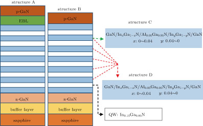
The structure of conventional InGaN-based LED (denoted as structure A) grown on a c-plane sapphire followed by a 2.5-μm thick GaN buffer layer, and a 0.5-μm thick layer of n-GaN:Si (5 × 1018 cm−3), is used as a reference in the study. There are six pairs of GaN/InGaN multiple quantum wells (MQWs) with 2-nm thick In0.15Ga0.85N wells and 11-nm thick GaN barriers in the active region. On the top of the MQW region is an 11-nm thick p-doped Al0.15Ga0.85N electron blocking layer (EBL): Mg (4 × 1017 cm−3) and 0.1-μm thick p-GaN:Mg (5 × 1017 cm−3). The second structure (denoted as structure B) has nothing different from structure A except the removal of the AlGaN EBL. In the third structure (denoted as structure C), the second-to-last GaN barrier is replaced by the GaN/InxGa1−xN/Al0.05Ga0.95N/InyGa1−yN/GaN barrier on the basis of structure B. The thickness values of the special barrier are 1 nm, 4 nm, 1 nm, 4 nm, and 1 nm respectively to keep the thickness of GaN barrier unchanged. The x increases from 0 to 0.04 and y decreases from 0.04 to 0 gradually. In the last kind of structure (denoted as structure D), the middle five barriers are the special barriers that are used in structure B and no EBL either. Concrete structures and relevant parameters about the four structures are shown in Fig.
The advanced physical model of semiconductor device simulation program (APSYS) is used to investigate the physical and optical properties of the four structures by solving the Poisson’s equation, the carrier transport equation, current continuity equations, the quantum mechanical wave equation and the photon rate equation. The area of the device geometry is 300 μm×300 μm. The Auger recombination coefficient and Shockley–Read–Hall (SRH) recombination time in quantum wells are set to be 1 × 10⁻³¹ cm6·s−1[19] and 100 ns, respectively in the simulation. To simplify the simulation, the operating temperature is set to be 300 K. The background loss is assumed to be 2000 m−1. The interface charge density is assumed to be 30% of the value calculated by the methods developed by Fiorentini[20] considering the fixed defects and other interficial charge. The parameters left can be found in Ref. [21].
Figure
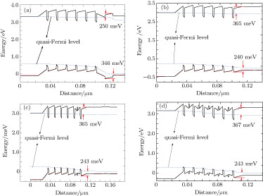 | Fig. 2. (color online) Calculated energy band diagrams of structure A (a), structure B (b), structure C (c), and structure D (d) at a current density of 350 A·cm−2. |
Figure
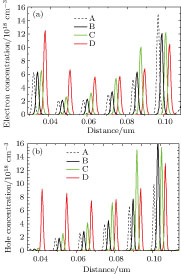 | Fig. 3. (color online) Carrier concentration for electron (a) and hole (b) at a current density of 350 A·cm−2 |
Because of the spontaneous and piezoelectric-polarization around the InGaN/AlGaN interface, polarization-induced charge will be formed around the interface. Associated with a gradient of polarization in space is a polarization-induced charge density given by ρ p = −𝑝. Here we consider the polarization along the [0001] axis, since this is the direction along which epitaxial film and InGaN/AlGaN heterostructures are grown both in reality and our simulation. The spontaneous polarization along the c axis of the wurtzite crystal is 𝑃SP = 𝑃SPz. The piezoelectric polarization can be calculated with the piezoelectric coefficients e33 and e13 (listed in the following Table
 | (1) |
 | (2) |
 | (3) |
Spontaneous polarization, piezoelectric constants of AlN, GaN, and InN.
| Wurtzite | AlN | GaN | InN |
|---|---|---|---|
| PSP/(C/m2) | −0.081 | −0.029 | −0.032 |
| e33/(C/m2) | 1.46[22] | 0.73[22] | 0.97[22] |
| e31/(C/m2) | −0.6[22] | −0.49[22] | −0.57[22] |
Measured and calculated elastic constants of wurtzite and cubic AlN, GaN, and InN.
| GPa Wurtzite | AlN | GaN | InN | |||
|---|---|---|---|---|---|---|
| exp. |
cal. |
exp. |
cal. |
exp. |
cal. |
|
| c11 | 34 | 396 | 374 | 367 | 190 | 223 |
| c12 | 125 | 137 | 106 | 135 | 104 | 115 |
| c13 | 120 | 108 | 70 | 103 | 121 | 92 |
| c33 | 395 | 373 | 379 | 405 | 182 | 224 |
| c44 | 118 | 116 | 101 | 95 | 10 | 48 |
experimental measured elastic constant of AlN (Tsubouchi et al.[23]);
calculated elastic constant (Wright[24]);
experimental measured elastic constant of GaN (Takagi Y et al.[25]);
experimental measured elastic constant of InN (Sheleg and Savastenko[26]).
Structural parameters, Bohr radii, and binding energies for AlN, GaN, and InN.[27]
| Wurtzite, 300 K | AlN | GaN | InN |
|---|---|---|---|
| a0/ Å | 3.112 | 3.189 | 3.54 |
| c0/ Å | 4.982 | 5.185 | 5.705 |
| c0/a0(exp) | 1.6010 | 1.6259 | 1.6116 |
Since [e31 −e33(c13/c33)] < 0 for AlGaN and InGaN over the whole range of compositions, the piezoelectric polarizations are negative for tensile and positive for compressive strained barriers, respectively. The spontaneous polarizations for GaN, AlN, and InN were found to be negative,[27] meaning that the spontaneous polarization points towards the substrate. As a consequence, the alignments of the piezoelectrical and spontaneous polarization are parallel in the case of tensile strain, and antiparallel in the case of compressively strained top layers, respectively.
A polarization sheet charge density can be determined by
 | (4) |
Here, we have a rough calculation on condition that the variation in none of composition, surface roughness, or strain distribution is taken into account to affect the distribution of polarization-induced sheet density. If the polarization-induced sheet charge density is positive (+σ), free electrons will tend to compensate for the polarization-induced charge. These electrons will form a 2DEG with a sheet carrier concentration, a negative sheet charge density (−σ) will cause an accumulation of holes, even a 2DHG at the interface.
Now we take InGaN/AlGaN (bottom/top) interface for example. To calculate the polarization-induced sheet charge density σ at the interface, we need to calculate the spontaneous and piezoelectric polarization in both the bulk material. First, for AlxGa1−xN, the spontaneous polarization and other parameters can be worked out by using the following set of liner interpolation between the physical quantities of GaN and AlN, i.e., piezoelectric polarization:
 | (5) |
lattice constant:
 | (6) |
elastic constants:
 | (7) |
 | (8) |
piezoelectric constant:
 | (9) |
 | (10) |
Then we need to know the spontaneous and piezoelectric polarization of the bottom InyGa1−yN. By analogy, we can obtain the spontaneous polarization of the InyGa1−yN:
spontaneous polarization:
 | (11) |
From Eq. (
 | (12) |
The piezoelectric polarization of AlxGa1−xN can also be calculated in the same method. Then the polarization-induced sheet charge density σ at the InGaN/AlGaN interface is
 | (13) |
 | (14) |
When x = 0.04 and y = 0.05, the polarization-induced sheet charge density σ at the InGaN/AlGaN interface is 0.01548 C/m2. The sheet charge σ/e is 0.967 × 10¹³ C/cm2. Similarly, the polarization-induced sheet charge density σ at the AlGaN/InGaN interface is −0.01522 C/m2. The sheet charge |σ/e| is 0.95 × 10¹³ C/cm2. So we believe that the 2DEG and DHG can form in the InGaN/AlGaN and AlGaN/InGaN interface as shown in Fig.
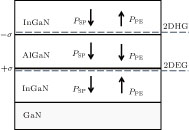 | Fig. 4. Polarization-induced sheet charge density and direction of the spontaneous and piezoelectric polarization in InGaN/AlGaN and AlGaN/InGaN heterostructure. |
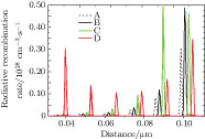
Figure
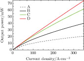
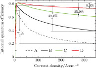
With the successful and effective modulation of the carrier distribution by the specially designed barriers, a great improvement in the light output power and IQE can be seen in Figs.
The effects of special barriers are studied numerically in this paper. Simulation results indicate that the LED with one designed GaN/InxGa1−xN/Al0.05Ga0.95N/InyGa1−yN/GaN barrier replacing the original GaN barrier is able to enhance the hole injections for the first five wells, especially for the adjacent wells, but release the holes in the last QW close to p-GaN side and improve the electron concentrations in the second-to-last QWs remarkably at the same time, meaning that the special barrier is quite useful to modulate the carrier concentrations in the two QWs adjacent to that barrier to a relatively close level. Additionally, with the adoption of the special barriers in all of the middle five QBs, a higher concentration and better uniformity of the carrier contribute to the higher radiative recombination rate, light output power, and lower efficiency droop.
| [1] | |
| [2] | |
| [3] | |
| [4] | |
| [5] | |
| [6] | |
| [7] | |
| [8] | |
| [9] | |
| [10] | |
| [11] | |
| [12] | |
| [13] | |
| [14] | |
| [15] | |
| [16] | |
| [17] | |
| [18] | |
| [19] | |
| [20] | |
| [21] | |
| [22] | |
| [23] | |
| [24] | |
| [25] | |
| [26] | |
| [27] |


