† Corresponding author. E-mail:
Project supported by the National Natural Science Foundation of China (Grant Nos. 11374219, 11474085, and 11534001) and the Natural Science Foundation of Jiangsu Province, China (Grant No BK20160007).
Disorder inevitably exists in realistic samples, manifesting itself in various exotic properties for the topological states. In this paper, we summarize and briefly review the work completed over the last few years, including our own, regarding recent developments in several topics about disorder effects in topological states. For weak disorder, the robustness of topological states is demonstrated, especially for both quantum spin Hall states with Z2 = 1 and size induced nontrivial topological insulators with Z2 = 0. For moderate disorder, by increasing the randomness of both the impurity distribution and the impurity induced potential, the topological insulator states can be created from normal metallic or insulating states. These phenomena and their mechanisms are summarized. For strong disorder, the disorder causes a metal–insulator transition. Due to their topological nature, the phase diagrams are much richer in topological state systems. Finally, the trends in these areas of disorder research are discussed.
Topological states, including gapped topological insulators and gapless topological semimetals, have become a focus of the condensed matter research.[1–8] In condensed matter systems, the first well-known insulating topological state is the quantum Hall effect (QHE) under a strong magnetic field.[9] Subsequently, the quantum anomalous Hall effect (QAHE), a topological state similar to the QHE but without magnetic field, was proposed in 1988[10] and observed in 2013.[11] In 2005, Kane et al. made a great step in the topological states research. They proposed the two-dimensional Z2 topological insulator, quantum spin Hall effect (QSHE) in graphene, which extends the topological state into the class of systems protected by time reversal symmetry.[12,13] Soon afterwards, the concept of symmetry protected topological states is broadened into three-dimensions[14,15] and other discrete symmetries.[7,16] Besides the insulating systems, the topological states can also exist in gapless systems.[17,18] More recently, topological semimetals, containing both Weyl semimetals and Dirac semimetals, were experimentally verified,[19–21] soon after they were predicted in the corresponding materials.[22–24] The topological states are different from normal metallic and insulating states because of the existence of nontrivial topological order, which originates from the global properties of all electrons below the Fermi energy[25] and can be characterized by various types of topological invariant numbers.[2,13,25] Due to the nontrivial topological order, corresponding gapless states emerge on the surface, leading to numerous exotic properties in topological systems. These properties have been reviewed in Refs. [1]–[8].
Experimentally, disorder is ubiquitous because of the defects in manufacturing processes and usually plays a dominant role in the transport properties of the samples being studied. Due to their unique electric structures, the response of topological states to disorder is fundamentally different from that in normal metals and insulators.[1,3,4,9,25–35] Physically, the topological invariant number can take on only a few discrete values. Therefore, the topological order cannot be easily disrupted by weak perturbations. That is to say, quantized transport that is robust against weak disorder can be obtained in various topological systems. Moreover, arising from their topological nature, topological states also show unconventional properties under moderate and strong disorder. Thus, studies of disorder effects can not only give a comprehensive understanding about topological states, but also offer a route map for the application of topological states. In this paper, based on several of our finished works in the last few years,[32–35] we briefly review three topics covered by recent studies of disorder effects in topological states. We note that there are other topics related to disorder, such as the weak anti-localization,[28,29] the chiral anomaly effects,[30,31] etc, which are not reviewed here.
The rest of this paper is organized as follows. In Section 2, the robustness of topological states against weak disorder is reviewed. In Section 3, we present how various types of disorder create topological insulator states from normal insulating or metallic states. In Section 4, the main results from studies of the metal–insulator transition in topological states systems are summarized. Finally, a brief conclusion and an outlook for future disorder research are given in Section 5.
Searching for material states with low-power dissipation is one of the greatest challenges in modern fundamental physics and materials science. In a real experimental sample, disorder always exists to some degree. A carrier propagating inside the sample will inevitably collide with disorder sites and be scattered. However, whether such a collision can cause energy dissipation depends on the ability of the scattering to induce backscattering processes–carriers propagating in the forward channel are scattered into the backward channel. In a normal metal, due to the spatial overlap between the forward and backward channels, backscattering can occur even for weak disorder. Therefore, the resistance (conductance) in a normal metal is not universal but in general increases (decreases) with the disorder strength. Transport in such a system is dissipative. In sharp contrast, in various kinds of topological systems, the spatial separation between the forward and backward channels and the existence of a special discrete symmetry (e.g., time-reversal symmetry) forbid backscattering.[36] As a result, carriers can propagate without dissipation. Thus, the resistance (conductance) in these systems is quantized and is insensitive to the presence of weak disorder. Such exotic phenomenon, namely the robustness of topological states, makes their host materials ideal platforms for testing fundamental physics principles and achieving low-power dissipation in electronic/spintronic devices.
That topological states are robust against weak disorder was first discovered in a milestone experiment on quantum Hall effects.[9] Klitzing et al. observed quantized Hall resistance and zero longitudinal resistance, independent of the material details. Subsequently, such phenomena have been extensively studied both within the context of the quantum Hall effect and in various other topological states.[37–43] In the following, as examples, we demonstrate the robustness of the topological states and the mechanisms of this behavior in two recently discovered systems: (i) quantum spin Hall effects (QSHE) in HgTe/CdTe quantum wells[32] and (ii) new proposed Z2 = 0 topological insulators with emerging robust helical surface states.[33]
For HgTe/CdTe quantum wells of moderate thickness, due to the strong spin–orbit coupling in this material, the system can enter a new topological phase–the QSH phase.[26,44,45] In Fig.
Next, in order to illustrate clearly the evolution of the conductance G versus disorder, the typical distributions of local currents in the device are plotted in Figs.
Topological insulators protected by time-reversal symmetry are characterized by the topological invariant number Z2.[13] There exist odd pairs of helical surface/edge states in topological insulators with Z2 = 1, which are robust and insensitive to material details and to external perturbations, as demonstrated in Fig.
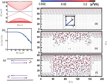 | Fig. 1. For a stripe geometry device with Fermi energy εF = 7 meV, and M = −10 meV. (a) Typical energy spectrum for a HgTe/CdTe quantum well strip in the QSHE region. (b) The conductance G versus disorder strength W in a two-terminal device. The Fermi energy is located inside the inverted gap. (c) Schematic of helical edge states propagation in the boundary of sample. On a given edge, the carriers with opposite spin polarizations propagate in opposite directions. (d)–(f) Configurations of the local current flow vector in a device with central region size Lx = 200a, Ly = 80a under disorder strength (d) W = 0, (e) W = 110 meV, and (f) W = 220 meV. The inset of panel (d) is the schematic of local current flow vector. The direction and length of the arrows represent the local current direction and magnitude. The order of magnitude of the local currents are displayed in the color bar. Adapted from Ref. [32] |
According to the popular view, Z2 = 0 topological systems have even pairs of helical surface/edge states, which are fragile in the presence of disorder.[42,48] However, we find that for some Z2 = 0 systems, robust transport can be engineered using a combination of finite size confinement and anisotropy.[33] With the help of the anistropic Bernevig–Hughes–Zhang (BHZ) model,[44,45] we demonstrate how robustness against disorder arises in such topological states.
In an anisotropic, Z2 = 0 BHZ stripe, for certain parameters, there are two pairs of helical edge states around k = 0 and k = π [Fig.
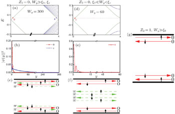 | Fig. 2. (a) and (d) One-dimensional energy bands for the 2D anisotropic BHZ stripe with Z2 = 0 and sample width Wy = 300 (a), 60 (d) described in the main text. Panels (b) and (e) show the distributions of edge states in real space corresponding to panels (a) and (d) with fixed Fermi energy. Panels (c) and (f) show schematic plots of helical edge modes corresponding to panels (a) and (d), respectively. The vertical arrows represent the electron spin. In panel (f), the helical edge channels around kx = π are hybridized due to finite size confinement, leaving one pair of helical edge channels around kx = 0. Thus, these conducting channels resemble the helical edge channels in a Z2 = 1 QSHE (g). Panels (c), (f), and (g) are adapted from Ref. [33]. |
 | Fig. 3. (a) and (e) Illustration of two-terminal and π-bar devices. The Anderson disorder exists only in the central (red) region. The size parameters are Lx = 120, Wx = 120, Wy = 60. (b)–(d) Two-terminal conductance G12,12 of the device in panel (a); (f)–(h) nonlocal conductance G14,23 of the device in panel (e) versus the Fermi energy εF for different disorder strengths W for the cases of a normal Z2 = 0 system (b) and (f); Z2 = 0 topological system with emergent robust helical edge states (c) and (g) and Z2 = 1 QSHE (d) and (h). G14,23 means that the current I14 is injected from terminal 1 to 4 and the voltage V23 is measured between terminals 2 and 3 and G14,23 = V23/I14. The error bars denote the conductance fluctuation. Adapted from Ref. [33]. |
In order to quantitatively assess the robustness of these emerging Z2 = 0 helical edge states, their transport properties under nonmagnetic disorder in a two-terminal device and a π-bar device [Figs.
Besides the anisotropic BHZ model, the Z2 = 0 topological systems involving helical surface states with emergent robustness have been extended into several 2D and 3D models.[33,49–51] In addition, two systems built on realistic materials: (i) Dirac semi-metal with appropriate width and thickness confinement[52] and (ii) a bismuth (111) film with a thickness of between 20 nm and 70 nm[33,53] are proposed to host robust helical surface states. Recent relevant experiments have shown the clues of the existence of such topological states in the latter proposed material system.[53,54] It is worth noting that the proposed Z2 = 0 systems have additional exotic properties not present in Z2 = 1 QSHE, which can be utilized to fabricate new topological devices.[52]
Besides destroying topological states, in special systems, moderate disorder can also produce topological states. The first well studied disorder induced topological state was the topological Anderson insulator (TAI). Specifically, in the clean limit, the system is in an ordinary insulator or metal. With the introduction of disorder, it enters into a topological insulator state with robust transport. This TAI was predicted to arise in HgTe/CdTe quantum wells by Shen’s group[55] and our group.[32] This type of TAI was then extended to many other systems.[56–67]
Let us begin with a review of how TAI arises in HgTe/CdTe quantum wells. In the clean limit, the system is described by the BHZ model[44]


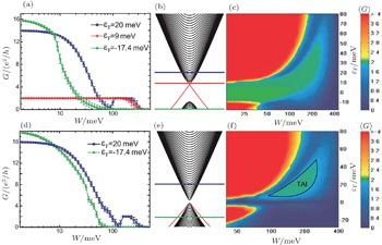 | Fig. 4. Conductance of disordered strips of HgTe/CdTe quantum wells. (a)–(c) and (d)–(f) Results for an inverted quantum well with M = −10 meV and for a normal quantum well with M = 1 meV, respectively. (a) The conductance G versus disorder strength W at three values of Fermi energy. The error bars represent the conductance fluctuations. (b) One-dimensional energy spectrum. The vertical scale (energy) is the same as that in panel (c) and the horizontal lines correspond to the values of the Fermi energy considered in panel (a). (c) Phase diagram showing the conductance G as a function of both disorder strength W and Fermi energy εF. Panels (d)–(f) are the same as panels (a)–(c), but for M > 0. The TAI phase is shown in the green region. In all panels, the strip width is 500 nm and the length is 5000 nm in panels (a) and (d), and 2000 nm in panels (c) and (f). Adapted from Ref. [55]. |
In Figs.
To validate this assumption, we study the evolution of the local current configurations under different disorder strengths [Fig.
Based on the discoveries described in Refs. [32] and [55], Groth et al. presented an effective medium theory that explains the physical origin of the TAI.[68] Disorder can induce self-energy Σ. In the self-consistent Born approximation (SCBA), Σ is given by[69]


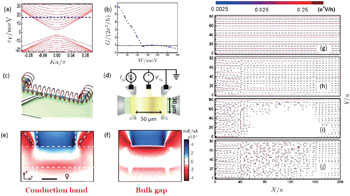 | Fig. 5. (a) Typical one-dimensional energy spectrum for a normal HgTe/CdTe quantum well strip. (b) Conductance G versus disorder strength W. (g)–(j) Configurations of the local current flow vector for the strip with the same sample sizes as for Fig. |
Groth et al.[68] found that the Anderson type of disorder [σ0,z] can make a negative correction [ReΣz < 0] to the topological mass M. Thus, it can lead to a transition of
If the effective medium theory is correct, one can deduce from Eq. (3) that the emergence of TAI is highly relevant to the type of disorder. Concretely, the σz term exists in 
To date, the physical properties of the TAI phase have been extensively studied,[71–77] and several significant advances are worth noting. In Figs.
In what follows, we introduce another type of topological state induced by disorder. Compared to the above TAI state, there are several differences. First, such a state is not triggered by the disorder strength but the randomness of the adatom configuration. Second, such a state cannot be explained by the effective medium theory. Third and of the greatest importance, contrary to the common view, such disorder-induced topological states are much easier to be realized than the normal insulator state in the periodic case.
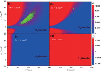 | Fig. 6. The conductance G ((a) and (b)) and renormalized topological mass |
Because of the outstanding properties of its electronic structure, graphene is considered as an ideal platform to host topological phases. For instance, recent first-principles calculations proposed that certain nonmagnetic adatoms (e.g., indium and thallium) could enhance the intrinsic spin–orbit coupling to give rise to the QSHE;[78–80] and some magnetic adatoms (e.g., 3d and 5d transition metals) could induce sizable Rashba spin–orbit coupling and magnetization to produce the quantized anomalous Hall effect (QAHE).[81–83] Though great theoretical progress has been achieved, no experimental observation has been reported. There are two major reasons preventing the experimental exploration of these novel states. (i) All the calculations are based on the periodic adsorption condition, which is beyond existing experimental capabilities. (ii) The formation of topological states is highly dependent on the adatom configurations. At certain coverage rates, the system is a trivial insulator.
Let us first explain why the topological nontrivial state and trivial insulator state can exist in the periodic adsorption case with different coverage rates. As illustrated in Figs.

The presence of the adatom at 𝓡 not only enhances the intrinsic SOC term (Hso) but also generates the on-site potential term (HU) with respect to the surrounding carbon atoms. Hso induces a topologically nontrivial gap Δso at both K and K′ with magnitude


When adatoms form a 
Interestingly, when the adatoms are nonuniformly distributed in space, the factor ei(K−K′)·𝓡 becomes randomized. As a result, even when the adatom is at the coverage rate 1/3n2 or 1/9n2, such randomization reduces ΔU from a large value in the periodical case to nearly zero in the random adsorption case. We note that the renormalization process for ΔU cannot be described by the effective medium case. In sharp contrast, the topologically nontrivial gap Δso is caused by zero momentum scattering. From Eq. (
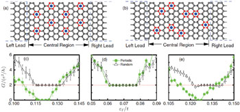 | Fig. 7. (a) and (b) Schematic of a two-terminal device with periodically and randomly distributed adatoms, respectively. Both adatom coverages are 11.1%. (c)–(e) Comparison of conductances G between periodic and random adsorption as a function of Fermi level εF. (c) and (d) The site potential and intrinsic SOC are set to U = 0.36t and λSO = 0.016t. The adatom coverages are 11.1% in panel (c) and 6.25% in panel (d). In panel (e) the magnetic adatoms coverage is 11.1%. Circle and triangle symbols represent the periodic and random adatoms. The error bars denote the conductance fluctuations. Adapted from Ref. [34]. |
As an example, we study the possibility of realizing QSHE states in graphene with randomly distributed adsorbates. Figure
The above adatom adsorption studies suggest that in a realistic graphene sample, the topological state is the favored ground state. Therefore, this calculation provides evidence of the high possibility of realizing topological phases in graphene.[34]
Since it was first proposed by P. W. Anderson, the disorder induced metal–insulator transition has been a long lasting, interesting research issue in condensed matter physics.[85] According to scaling theory, the metal–insulator transition in a material system depends on its universality ensemble [symplectic, unitary and orthogonal] and dimension.[86–88] Initially, it was believed that the extended states (metal) could exist only in three-dimensional systems and that all the bulk states in two and one-dimensional systems were localized (insulator).[86] Later, two exceptions were found in two-dimensional systems. One was the system with strong spin–orbital coupling [symplectic ensemble]. The other was a system without time reversal symmetry [unitary ensemble]. The topological states always share these two features and then become the focus of research on the metal–insulator transition. In the past two decades, the metal–insulator transition in quantum Hall systems has been clearly understood.[89–91] The extended state can only exist at the transition point between different plateaus. The critical exponents of the transition have also been obtained. In the last few years, there have been many studies of the metal–insulator transition in a QSHE.[92–96] Their results can be summarized as follows: (i) for a QSHE with Rashba spin–orbital coupling, the system belongs to a sympletetic ensemble. A metallic phase emerges between the QSH phase and the normal insulator phase; (ii) for a QSHE without Rashba spin–orbital coupling, the system can be divided into two spin subsystems, both of which belong to unitary ensemble. A direct transition from a QSHE to a normal insulator is observed. Though the metal–insulator transition in two-dimensional topological states has been extensively studied, the transition properties in three-dimensional topological states are still not quite clear.
More recently, the Weyl semimetal (WSM), a gapless topological state in three-dimensions, has been theoretically predicted and experimentally confirmed.[18–20,22] Thus, it is timely to study the effects of disorder and metal–insulator transition both for their direct experimental relevance and for their fundamental value in advancing the understanding of the interplay between randomness and topological order. In Ref. [35], we do so by using both numerical and analytical approaches. Different from the previous studies that only concentrate on a single weyl node,[97–99] we focus on a more realistic tight-binding model with considering the interplay of opposite weyl nodes.[100,101] By calculating the localization length [102] and the Hall conductivity,[103,104] we obtain the complete phase of the system under all the disorder strength. Because the WSM has novel gapless excitations, i.e., the Weyl nodes in the bulk and Fermi arcs on the surface, we find an unexpected rich phase diagram, as shown in Fig.
It is worth noting that independent of our work, Liu et al. also studied the disorder induced metal–insulator transition in 3D QAH layer systems and observed a rich phase diagram.[105] Moreover, the unconventional WSM to metal transition has also generated broad interest, and the critical exponent of the transition has been obtained.[105–107]
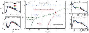 | Fig. 8. (a), (b), (d), and (e) Normalized localization length Λ = λ (L)/L versus disorder strength W for different masses mz [lines in panel (c)], λ(L) is the localization length of a long bar sample with cross section L × L. An increase in Λ with L signals a metal phase, while a decrease with L signals an insulator phase. When Λ is independent of L, this signals a critical point of the phase transition. (c) Phase diagram in the W–mz plane. The symbols guided by the solid lines were obtained from the normalized localization length. The dashed blue lines are the phase boundaries determined using the SCBA. In a finite layer sample, the 3D QAH, WSM and diffusive anomalous Hall metal phases are distinguished by its Hall conductance being quantized and equivalent to layer number, being quantized, and being non-quantized, respectively. Adapted from Ref. [35]. |
In this paper, based on reviewing our own disorder studies and other relevant works produced over the last few years, recent developments into the effects of disorder in topological states are briefly summarized. We show that all weak, moderate and strong disorder can lead to exotic phenomena in various types of topological states. How these phenomena originate from the topologically nontrivial nature of topological states is also demonstrated. In spite of significant recent progress, there is nevertheless still plenty of room for further research into the effects of disorder in topological states. Before concluding the review, we discuss the opportunities for disorder studies in the future.
Experimental and material realization of disorder related topological phases. Seven years after its first prediction,[32,55] the first signs of the experimental realization of the TAI phase have now been found. However, the host system is evanescently coupled waveguides.[57,108] Due to the recent great advance in controlling the disorder strength[109] and in the measurement of the local current[110] in topological material, we expect the TAI phase can soon be confirmed in condensed matter systems. It is also to be noted that the topological phase in graphene has promising applications in information processing. We have demonstrated that both QSHE and QAHE states in graphene can easily be engineered through randomly adsorbing nonmagnetic/magnetic adatoms.[34] We also expect the experimental observation of these topological states.
Understanding the fundamental phenomena caused by the disorder. Our understanding of many disorder related phenomena is still limited. Firstly, it is a common belief that the 2D unitary system is scaled to insulator except at some isolated critical points.[88] However, in Refs. [111] and [112], though the considered models are totally different, we find in both a novel metallic phase region that may emerge between QSHE and normal insulator phases. The physical origins for the metallic phase and the relationship between these two models should also be carefully addressed. Secondly, analogue to disorder induced Anderson localization benefits the observation of quantized Hall plateaus in QHE, the disorder also plays an important role in the experimental observation of the QSHE and QAHE.[46,47] Du et al. found that dilute silicon impurity doping in InAs/GaSb quantum wells can greatly suppress residual bulk conductance and produce a perfect QSHE.[47] From the point of view of theory, despite the attempt to study the phenomena,[59] the mechanism for the effects of impurity doping on the transport properties of the system is still not clear. Significantly, there exist great puzzles regarding disorder effects in thin films of chromium-doped (Bi,Sb)2Te3, which is key to understanding why the QAHE can only be observed at extremely low temperatures.[11,113] Thirdly, type-II Weyl semimetals, which harbor unconventional Weyl nodes, have been proposed recently.[114] It would be interesting to study the stability of these Weyl nodes under strong disorder. Finally, dephasing effects also exist in realistic samples. A natural topic is how the transport properties of topological states are affected when both disorder and dephasing effects are considered.[115]
| 1 | |
| 2 | |
| 3 | |
| 4 | |
| 5 | |
| 6 | |
| 7 | |
| 8 | |
| 9 | |
| 10 | |
| 11 | |
| 12 | |
| 13 | |
| 14 | |
| 15 | |
| 16 | |
| 17 | |
| 18 | |
| 19 | |
| 20 | |
| 21 | |
| 22 | |
| 23 | |
| 24 | |
| 25 | |
| 26 | |
| 27 | |
| 28 | |
| 29 | |
| 30 | |
| 31 | |
| 32 | |
| 33 | |
| 34 | |
| 35 | |
| 36 | |
| 37 | |
| 38 | |
| 39 | |
| 40 | |
| 41 | |
| 42 | |
| 43 | |
| 44 | |
| 45 | |
| 46 | |
| 47 | |
| 48 | |
| 49 | |
| 50 | |
| 51 | |
| 52 | |
| 53 | |
| 54 | |
| 55 | |
| 56 | |
| 57 | |
| 58 | |
| 59 | |
| 60 | |
| 61 | |
| 62 | |
| 63 | |
| 64 | |
| 65 | |
| 66 | |
| 67 | |
| 68 | |
| 69 | |
| 70 | |
| 71 | |
| 72 | |
| 73 | |
| 74 | |
| 75 | |
| 76 | |
| 77 | |
| 78 | |
| 79 | |
| 80 | |
| 81 | |
| 82 | |
| 83 | |
| 84 | |
| 85 | |
| 86 | |
| 87 | |
| 88 | |
| 89 | |
| 90 | |
| 91 | |
| 92 | |
| 93 | |
| 94 | |
| 95 | |
| 96 | |
| 97 | |
| 98 | |
| 99 | |
| 100 | |
| 101 | |
| 102 | |
| 103 | |
| 104 | |
| 105 | |
| 106 | |
| 107 | |
| 108 | |
| 109 | |
| 110 | |
| 111 | |
| 112 | |
| 113 | |
| 114 | |
| 115 |


