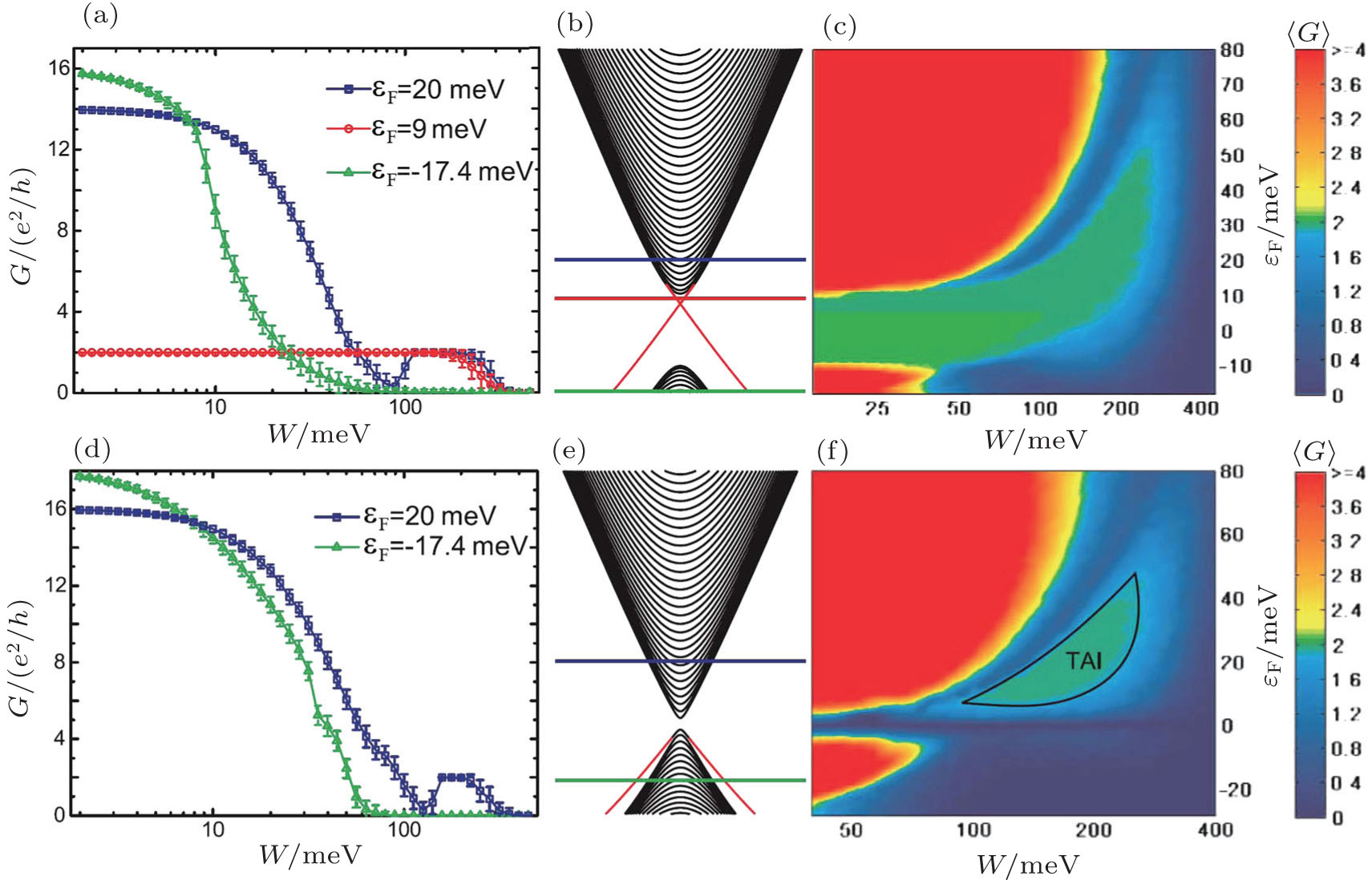
Conductance of disordered strips of HgTe/CdTe quantum wells. (a)–(c) and (d)–(f) Results for an inverted quantum well with M = −10 meV and for a normal quantum well with M = 1 meV, respectively. (a) The conductance G versus disorder strength W at three values of Fermi energy. The error bars represent the conductance fluctuations. (b) One-dimensional energy spectrum. The vertical scale (energy) is the same as that in panel (c) and the horizontal lines correspond to the values of the Fermi energy considered in panel (a). (c) Phase diagram showing the conductance G as a function of both disorder strength W and Fermi energy εF. Panels (d)–(f) are the same as panels (a)–(c), but for M > 0. The TAI phase is shown in the green region. In all panels, the strip width is 500 nm and the length is 5000 nm in panels (a) and (d), and 2000 nm in panels (c) and (f). Adapted from Ref. [55]. |

