


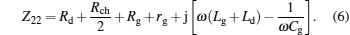
Small-signal modeling of GaN HEMT switch with a new intrinsic elements extraction method
[Geng Miao1, 2, Li Pei-Xian1, Luo Wei-Jun2, Sun Peng-Peng2, Zhang Rong1, 2, Ma Xiao-Hua1, †,  ]
]
]
|
|


† Corresponding author. E-mail:
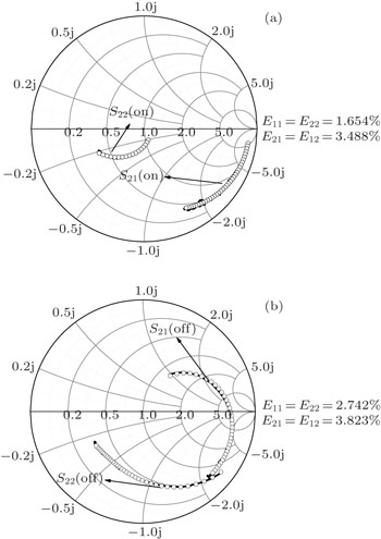
A novel and accurate method is proposed to extract the intrinsic elements of the GaN high-electron-mobility transistor (HEMT) switch. The new extraction method is verified by comparing the simulated S-parameters with the measured data over the 5–40 GHz frequency range. The percentage errors Eij within 3.83% show the great agreement between the simulated S-parameters and the measured data.
Radio frequency (RF) switches play an important role in modern communication systems such as mobile base station transceivers and satellite communication transmitters. Currently, the two most widely used microwave and RF semiconductor components in switches are PIN diodes and GaAs metal–semiconductor field effect transistors (MESFETs).[1] The traditional PIN diode based T/R switches encounter additional losses as a result of their intrinsic DC power consumption. The GaAs FET-based switches are hampered by the relatively low breakdown voltage of the components, which require multi-stage design configurations with active device series connections to divide the maximum voltage of the input signal.[2] The GaN on silicon carbide (SiC) HEMT technology offers many advantages over the existing GaAs technology.[3–5] Because of its higher breakdown voltage, GaN promises to extend the power level of the FET-based microwave circuits by at least a factor of five.[6–8] The greatly increased breakdown voltage (VBD) will allow the use of a higher control voltage and correspondingly larger RF voltage swings for off-state transistors. The high maximum current capability (IMAX) reduces the channel resistance and increases the RF current swing for on-state devices. The insulating SiC substrate reduces the substrate leakage due to the high RF voltage swing and improves heat transfer to the backside of the MMIC.[9] Furthermore, GaN HEMT switches can provide low insertion loss and high switching speed performance with minimal dc-bias power needed for the switching action. It also enables excellent small and large signal performances over a wider frequency band. This has positioned the GaN HEMT based RF switches as the natural replacement for the Si PIN diode or GaAs PHEMT switches with more application space to be explored.
Over the last few decades, the development of an accurate device model has proven to be a vital step in the “first pass” design approach. As we know, an accurate extraction method for a proper small-signal equivalent circuit is vital for designing circuits, evaluating the process technology, and optimizing the device performance. However, modeling switches is not as extensively covered in some previous literatures as that of a power amplifier (PA). Also, switches usually operate at passive mode and in practice in a common gate (CG) configuration, which is different to the familiar common source (CS) model.[10] So far, there is almost no detailed extraction procedure for the GaN HEMT switch model in the previous publications.
We propose a new method for the extraction of the intrinsic elements in the GaN HEMT switch and describe the whole extraction procedure of elements in the GaN HEMT switch model. In Section 2, the device structure is presented. The detailed extraction procedure of the extrinsic and intrinsic elements is described in Section 3. In Section 4, the results and validity of the proposed small-signal modeling procedure are discussed. Finally, some concluding remarks are given in Section 5.
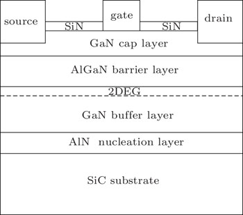
The GaN based HEMT switch employed in this work is grown on a SiC substrate as shown in Fig.
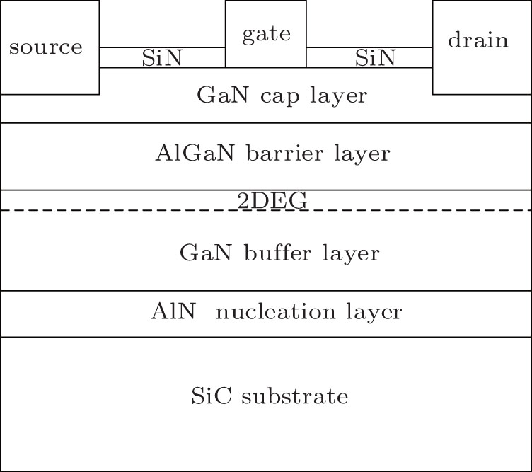 | Fig. 1. Cross-sectional structure of GaN based HEMT switch. |
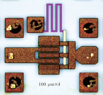
 | Fig. 2. GaN based HEMT switch with gate size of 4 × 100 μm. |
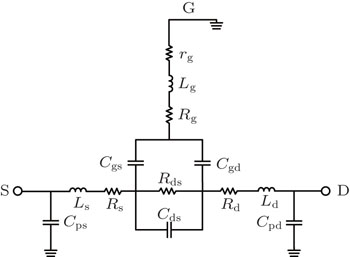
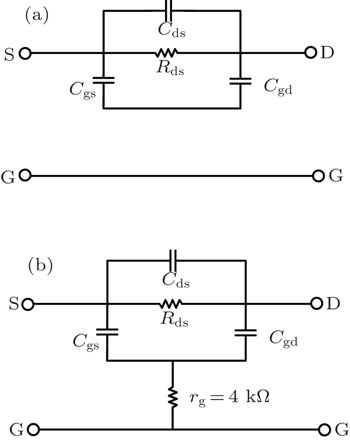
Based on the physical properties, the schematic of the AlGaN/GaN HEMT equivalent circuit is shown in Fig.
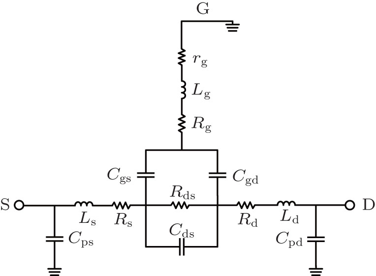 | Fig. 3. Small signal equivalent circuit of GaN HEMT switch. |
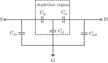
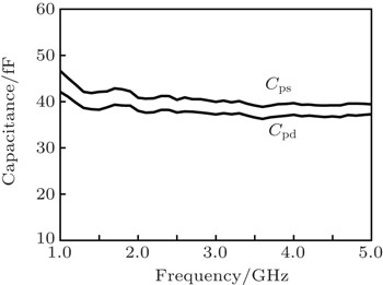
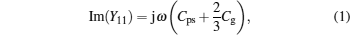
Parasitic source and drain pad capacitances of GaN HEMT are generally extracted by the conventional cold pinch-off (VDS = 0 V, VGS < Vp) techniques. Under the condition VGS < Vp, the channel between the source and the drain is completely pinched-off with the capacitive elements dominant. At low frequencies, the inductances and resistances can be neglected as they do not influence the imaginary part of the Y parameters. At VDS = 0 V, the depletion layer under the gate is symmetric and this allows us to assume that Cgs and Cgd equal to Cg. Such an approximation depends on the symmetric structure of the switch device. Under this bias state, the equivalent-circuit topology of Fig.


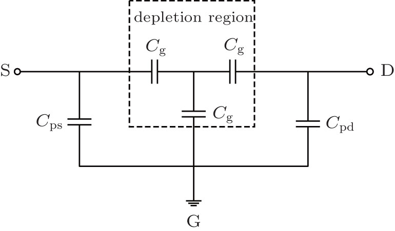 | Fig. 4. Cold pinch-off equivalent circuit for GaN HEMT at low frequency. |
The extracted parameters via Eqs. (
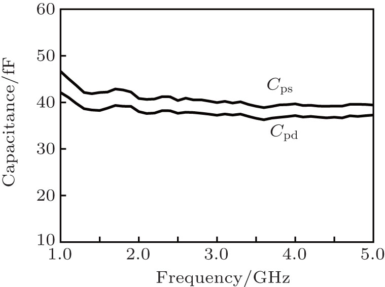 | Fig. 5. Extracted pad capacitances against frequency. |
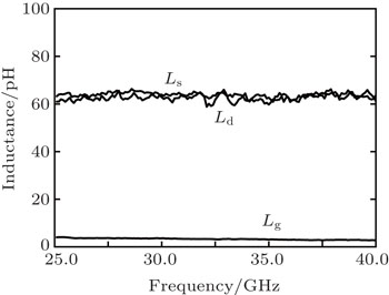
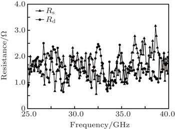
After de-embedding the effect of the pad capacitances, the other six extrinsic elements can be determined from Z-parameters under no bias condition in Fig.
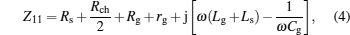

As illustrated in Eqs. (

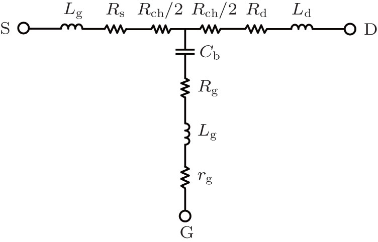 | Fig. 6. Equivalent circuit for the GaN HEMT under no bias condition. |
Figure
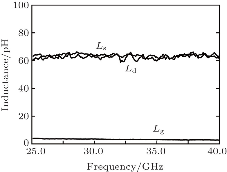 | Fig. 7. Extracted feed line inductances against frequency. |
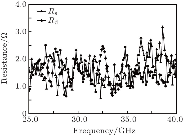 | Fig. 8. Extracted extrinsic resistances against frequency. |
| Table 1. Extracted extrinsic elements of device with gate size of 4×100 μm. . |
Usually, the Y parameters of common source devices satisfy Y11 ≠ Y12 ≠ Y21 ≠ Y22. There is only a small ohmic contact resistance between the source and the ground. After de-embedding all the parasitic parameters, the intrinsic part of the CS device can be obtained directly by the Y parameters of the two-part network. In the same way, for the CG GaN HEMT switch device, after de-embedding the extrinsic parameters, the intrinsic part is shown in Fig.

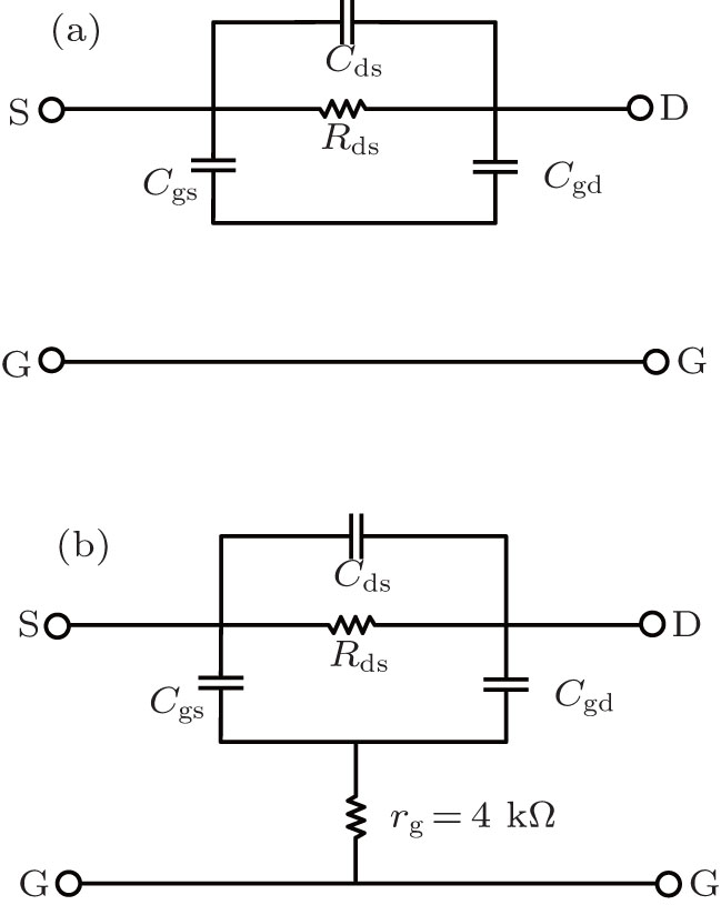 | Fig. 9. The intrinsic part (a) without rg and (b) with rg. |
The GaN HEMT under switch bias condition is passive, and hence, the condition Y12 = Y21 is satisfied in Eq. (
So far, the previous literatures have not given any specific equations of the extraction method about the intrinsic parameters in switch models. Most of the intrinsic parameters were extracted by optimization or some algorithms.[16–21] Based on the problem mentioned above, a specific method and a detailed procedure of intrinsic parameters extraction are described as follows.
As shown in Fig.
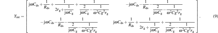
The Y parameters in matrix (


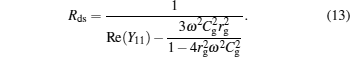
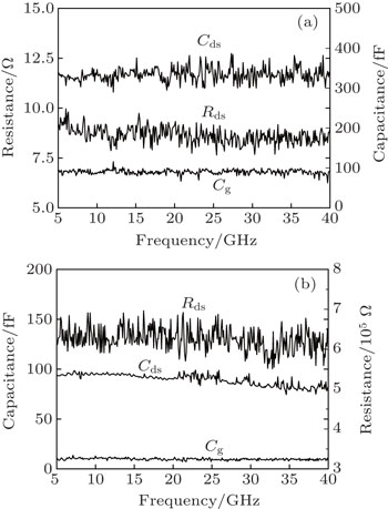
The introduction of the blocking resistor during the extraction of the intrinsic parameters in the GaN HEMT switch adds another two equations about the intrinsic elements. Four equations correspond to four unknowns. Figure
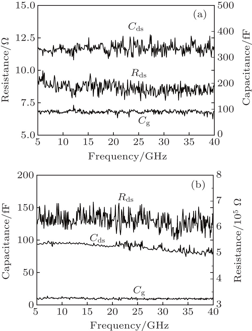 | Fig. 10. Extracted Cds, Rds, Cg versus frequency: (a) on state, (b) off state. |
| Table 2. Intrinsic elements of GaN HEMT switch with gate size of 4×100 μm. . |
The process described above has been used to model the GaN HEMT switch over a frequency range from 5 GHz to 40 GHz. The devices have 0.25 μm gate length, 100 μm finger pitch, and 200 μm, 400 μm, or 800 μm gate size. Furthermore, the CG GaN HEMT switch has a geometric symmetry which is reflected in the observation that S11 ≈ S22 and S12 ≈ S21. Figure
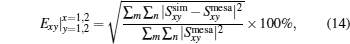
 | Fig. 11. Comparisons of S-parameters between measurement (—) and simulation (°) in a frequency range of 5–40 GHz for a device with gate size of 4 × 100 μm: (a) S21, (b) S22. |
The agreement between the measured and the modeled S parameters is very good. The percentage errors Eij between the measured and the modeled Sij parameters are within 3.85%. As we know, the S parameters of the GaN HEMT switch are changed with the gate size. In the actual MMIC design, an optimum gate width is determined according to the need of circuit performance. Therefore, we model the switching devices with different gate sizes, and outline their intrinsic parameters at on and off states in Table
| Table 3. Intrinsic parameters of GaN HEMT switches with different sizes. . |
| Table 4. The error percentage of different size GaN HEMT switches. . |
As can be seen from the extracted parameters, with the increase of the gate width, the on state resistance (Ron = Rs + Rds + Rd) decreases, and the cut-off capacitance (Coff = Cgs + Cds + Cgd) increases. The on state resistance Ron directly affects the insertion loss, while the cut-off capacitance Coff affects the isolation. There is no certain relationship between the cut-off resistance Roff and the gate size. This is because when Roff is larger than a certain value, its influence on the performance of the switch can be ignored. The product of Ron · Coff is constant and independent of the total transistor gate size.
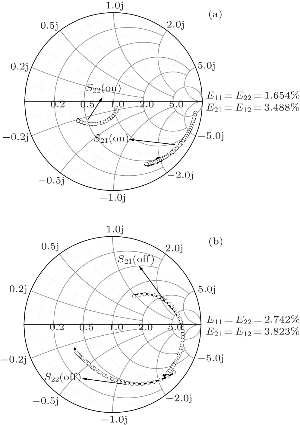
The circuit topology and micrograph of an x-band SPDT switch are shown in Fig.
 | Fig. 12. (a) Circuit topology and (b) micrograph of the x-band AlGaN/GaN SPDT power switch. |
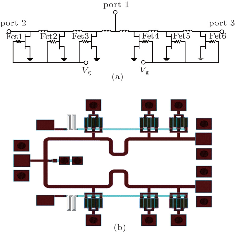
The comparisons between the simulated and the modeled results of insertion loss and isolation are presented in Fig.
 | Fig. 13. Simulated and modeled insertion loss and isolation of the x-band switch. |
The small-signal equivalent circuit model for understanding the physical structure and predicting small signal S parameters of a device is useful, but it cannot reflect the large signal corresponding RF power harmonic characteristics.[26] Therefore, the large signal model of the GaN HEMT switch is also of great importance. For the design of switches, the nonlinear model can predict the I–V curves at both positive and negative drain–source voltages, and particularly the continuity of the current in the proximity of Vds = 0 V. It can also provide an accurate estimation of the output power as well as the power added efficiency (PAE).[27] As a result, there is a crucial need for developing a dedicated nonlinear model for the GaN HEMT switch from widely used DC and S-parameter measurements, which can be used for successful first-pass design.
A novel and accurate direct extraction method of the intrinsic elements of the GaN HEMT switch has been presented. The frequency independence of the extracted intrinsic elements confirms that the intrinsic elements are extracted accurately. This technique is verified through the agreement between the measured and the modeled S-parameters under different bias conditions. Good agreement is obtained between the modeled and the measured results for different gate size HEMTs. The proposed method would be useful for determining the intrinsic elements of the GaN HEMT switches.
| 1 | |
| 2 | |
| 3 | |
| 4 | |
| 5 | |
| 6 | |
| 7 | |
| 8 | |
| 9 | |
| 10 | |
| 11 | |
| 12 | |
| 13 | |
| 14 | |
| 15 | |
| 16 | |
| 17 | |
| 18 | |
| 19 | |
| 20 | |
| 21 | |
| 22 | |
| 23 | |
| 24 | |
| 25 | |
| 26 | |
| 27 |