† Corresponding author. E-mail:
Project supported by the National Basic Research Program of China (Grant No. 2014CB339900) and the Open Fund of Key Laboratory of Complex Electromagnetic Environment Science and Technology, China Academy of Engineering Physics (CAEP) (Grant No. 2015-0214.XY.K).
An electromagnetic pulse (EMP)-induced damage model based on the internal damage mechanism of the GaAs pseudomorphic high electron mobility transistor (PHEMT) is established in this paper. With this model, the relationships among the damage power, damage energy, pulse width and signal amplitude are investigated. Simulation results show that the pulse width index from the damage power formula obtained here is higher than that from the empirical formula due to the hotspot transferring in the damage process of the device. It is observed that the damage energy is not a constant, which decreases with the signal amplitude increasing, and then changes little when the signal amplitude reaches up to a certain level.
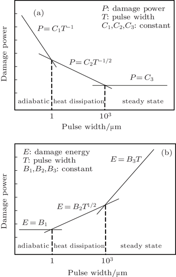
With the increasingly complicated electromagnetic environment, the electromagnetic pulse (EMP) threat to semiconductor devices has received growing attention in recent years.[1,2] It is important to make a reasonable estimate of whether or not the device will be damaged by EMP events. Such a prediction requires a knowledge of the damage threshold. There has been extensive work done in this aspect. Wunsch and Bell investigated the pulse power damage level of a semiconductor junction, and developed a semi-empirical formula based on the thermal failure model and extensive experimental data.[3] Tasca divided the damage level into three domains by the pulse width, i.e., the short pulse under the assumption of adiabatic condition, the longer pulse with considering heat loss which is similar to the Wunsch–Bell model,[3] and the steady state phase with thermal equilibrium established.[4] All these researches assumed the device to be a fixed heat source to study the EMP-induced damage threshold, and did not consider the internal physical mechanism of the device. So, uncertainties and errors associated with these models existed in EMP assessment and hardening design.[5] With the size of the device getting smaller, these uncertainties and errors become more and more serious. It is desired to find the relationship between the damage threshold and damage mechanism of the device. However, very few data have been presented in the literature in this aspect to date.[6]
The present study on the damage threshold of devices is completely different from that from the conventional method based on a simple thermal model. It establishes directly the damage model with the realistic damage process of the GaAs PHEMT device injected by EMP. Based on this model, the damage thresholds with terms of the damage power and damage energy are investigated. In addition, adopting the curving fit method, the GaAs PHEMT damage power formula related to the pulse width is also established.
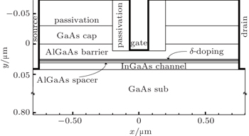
Figure
Presently, the researchers mostly take the step voltage pulse as the signal model in the study of the damage effect of the semiconductor device with the EMP event.[7–9] In this work, a step voltage pulse with a rising time of 0.1 ns and amplitude of 9 V is applied to the gate electrode of the device, in which the other two electrodes are biased at 2 V on the drain and grounded on the source, respectively. With the help of the device simulation software Sentaurus TCAD, the internal physical behavior of the device injected with pulse signal is simulated by solving the Poisson equation, the carrier continuity equation, the carrier temperature and heat flow equations. Here, we take the lattice temperature reaching 1511 K, the melting point of GaAs, as the damage criterion of the device.
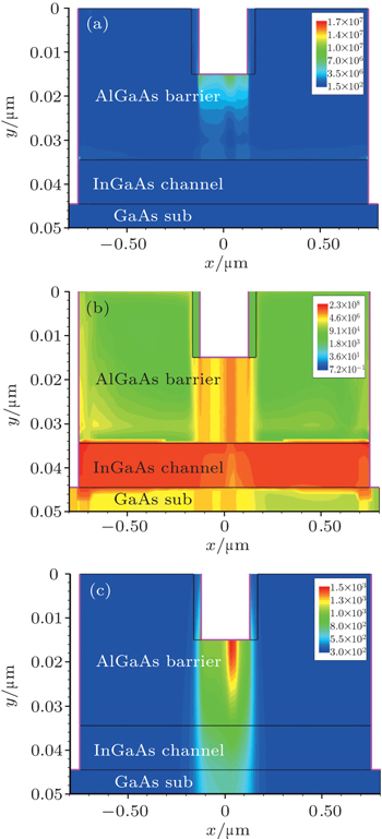
When the device is subjected to step voltage pulse on the gate electrode, there is a current path emerging between the gate and the InGaAs channel due to the Schottky barrier being lowered. Considering the potential differences between the gate, source and drain, the current path is closer to the source and the maximum electric field is located below the gate near the source, which then leads to the temperature distribution of the device (Fig.
 | Fig. 2. Distributions of the device parameters: (a) current density (A/cm2), (b) electric field (V/cm), and (c) temperature (K), at t = 0.08 ns. |
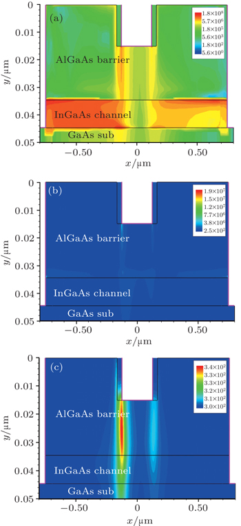
 | Fig. 3. Distributions of the device parameters: (a) hole density (cm−3), (b) electric field (V/cm), and (c) current density (A/cm2), at t = 0.25 ns. |
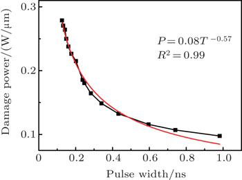
Generally, the EMP-induced damage effect on the device is divided into three cases by the pulse width:[3,4,11] for the short pulse on the assumption that the device is adiabatic, for the long pulse with considering heat dissipation, and for the steady state with thermal equilibrium established. Figure


In order to analyze the damage threshold of the GaAs PHEAT, such as the damage power, damage energy, we simulate the burnout process of the device with different amplitudes of step voltage pulse based on the damage model illustrated in Section 2. Here, the pulse width is the duration time of injection signal before the device is burnout, the damage power is the average power absorbed by the device, and the damage energy is determined by calculating the instantaneous voltage and current waveform on the device each as a function of the pulse width.
 | Fig. 5. Variation rules of the damage threshold ((a) damage power and (b) damage energy) with pulse width. |
Figure

From the comparison between formulas (
From the analysis in Subsubsection 2.3.1, it is noted that the device damage belongs to energy-induced damage under the injection of EMP. Figure
Reference [12] shows the HPM induced injection experiment on the GaAs PHEMT. Subjected to the microwave signals is the gate electrode of the device, which has the same structure as that in Subsection 2.1. Experimental results show that both positions beneath the gate near the drain and source could possibly be damaged (Fig.
 | Fig. 9. Photomicrographs of damaged devices: (a) sample 11# and (b) sample 12#, with microwave pulse.[12] |
Here it should be pointed out that although the injection signal in this work is different from the one in Ref. [12], damages induced by both the step voltage pulse and microwave pulse are both energy dependent processes,[13] which has a certain similarity, i.e., they have the same structures and injection locations. The good agreement between the simulation results and experimental results implies that the damage model established here can predict the damage effect of EMP-induced injection on the GaAs PHEMT well.
It is necessary to have a knowledge of the damage threshold in the EMP assessments and hardening designs. The method used in this study is distinctively different from the traditional method of the threshold study that is based on the thermal model: here we directly use the damage effect and mechanism of the typical device as the damage model. It is demonstrated that the empirical formula P = C1T− 1 should be modified into P = P = C1T−0.57 for the GaAs PHEMT due to the hotspot shifting in the damage process of the device. Because the damage position varies with the amplitude of injection signal, the damage energy is not a constant, which is different from the empirical viewpoints. It should be noted that in this paper we only investigate the difference between the damage threshold obtained from the empirical viewpoint and that from the simulation analysis. In the future research, the experiment data will also be considered to fit the damage power formula with the pulse width index obtained in this paper.
| 1 | |
| 2 | |
| 3 | |
| 4 | |
| 5 | |
| 6 | |
| 7 | |
| 8 | |
| 9 | |
| 10 | |
| 11 | |
| 12 | |
| 13 |


