† Corresponding author. E-mail:
‡ Corresponding author. E-mail:
Project supported by the National Natural Science Foundation of China (Grant Nos. 91321310, 11274156, 11474152, 11474153, 61521001, and 11504165) and the State Key Basic Research Program of China (Grant Nos. 2011CB922104 and 2011CBA00205).
We fabricate high-quality Al/AlOx/Al junctions using improved bridge and bridge-free techniques at 30-keV e-beam voltage, in which the length of undercut and the size of junction can be well controlled by the pre-exposure technique. The dose window is 5 times as large as that used in the usual Dolan bridge technique, making this technique much more robust. Similar results, comparable with those achieved using a 100-keV e-beam writer, are obtained, which indicate that the 30-keV e-beam writer could be an economic choice for the superconducting qubit fabrication.
As a nonlinear element, the Josephson junction is the key component of many superconducting electronic devices such as the superconducting quantum interference device (SQUID),[1] rapid single flux quantum (RSFQ),[2] single electronic transistor (SET),[3] Josephson parameter amplifier (JPA),[4] and superconducting quantum bit (qubit).[5] With the rapid development in the last twenty years, supconducting quantum computing (SQC) is regarded as a promising candidate to realize a practical quantum computer. As a foundation of SQC, the reliability and reproducibility of qubit fabrication are important, especially for its scaling. Owing to its long coherence time and simple fabrication process, the Al/AlOx/Al junction is used by many SQC groups nowadays.[6–14] Among different kinds of fabrication processes of the aluminum junction, the Dolan bridge technique is widely adopted because it only needs one lithographic patterning step[15] in which a suspended bridge is formed via a different clearing dose of the bilayer resist. After two-angle aluminum film depositions and an in-situ oxidation in electron beam evaporator, the Al/AlOx/Al junction is prepared. Although this fabrication process is simple, its robustness is not optimistic since the suspended bridge formed by the different clearing dose of bilayer resist is frail. Due to the instability of e-beam, the variation of resist thickness, and its denaturation, the size and reproducibility of the junction can be easily changed and affected.
To overcome these problems, the Martinis group[16] and Buission group[17] have proposed an improved fabrication technique (here named the pre-exposure technique). In contrast to the usual Dolan bridge fabrication, the pre-exposure technique has two lithographic steps. The first one writes the bottom layer and the second one writes the top layer to define the junction pattern. Unlike the traditional technique, the suspended bridge is not formed by self-acting, which results from the different clearing dose of bilayer resist, but by the intended pre-exposure. Using this technique, high reproducibility of aluminum junctions with well-defined size can be achieved. It should be emphasized that in both pre-exposure techniques mentioned above, 100-keV acceleration voltage of e-beam is used. Under such a high e-beam voltage, the forward scattering is mainly suppressed and the e-beam with low pre-exposure dose (for bottom layer writing) has little effect to the top layer.
Can this technique be applied using the 30-keV e-beam writer, which is widely used and often built up with a 30-keV e-beam voltage scanning electron microscope (SEM) and a pattern generator? Compared with the 100-keV e-beam writer, the 30-keV e-beam writer usually has a larger forward scattering effect on the bilayer resist, which makes the applicability of the pre-exposure technique uncertain. In this paper we present a systematic study of the pre-exposure technique using a 30-keV e-beam writer and demonstrate that similar results can be obtained as in the case using the 100-keV e-beam writer. High-quality aluminum junctions with area ranging from 0.04 μm2 to 10 μm2 are fabricated. The clearing dose window of this technique extends to 5 times (400 μC/cm2–600 μC/cm2) as large as that used in the traditional Dolan bridge technique (440 μC/cm2–480 μC/cm2), making it more robust for the junction fabrication.
The 30-keV E-beam writer used in the present work is a field emission SEM (Inspect F50 from FEI) equipped with a pattern generator (Raith), with the beam current variable between several pico-amperes and hundreds of nano-amperes depending on the selected spot size. To define the nano-scale pattern more accurately, we choose a small spot size with beam current around 20 pico-amperes. The working distance is 5.5 mm from e-gun to sample stage. We use high resistivity silicon substrates whose thinkness is 0.5 mm. The e-beam bilayer resists are PMMA950 A3 and MMA(8.5)MAA EL13 from the MicroChem company, which will be called PMMA and MAA below, respectively, for simplicity.
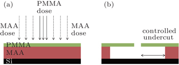
The bottom layer (MMA) is spun at 3000 rpm for 1 minute (thickness is around 600 nm) and baked at 170 °C for 3 minutes. The top layer (PMMA 950 A3) is spun at the same speed and time (thickness is around 200 nm), also baked at 170 °C for half an hour. In the traditional technique, during the exposure of e-beam at PMMA dose, high energy electrons break the bonds of PMMA and increase its solubility in the developer. The MAA polymer is much more sensitive to electrons, thus it dissolves much faster in the developer, resulting in the undercut underneath the top polymer layer. If two exposed areas are close together, the bottom layer under them will be fully developed to form a hanging bridge of the top layer, namely the Dolan bridge.
It is worth noting that the length of undercut of the Dolan bridge is formed by the different sensitivity of bilayer to e-beam which is hard to be controlled arbitrarily. For example, we need a higher e-beam dose to achieve a longer undercut. At such high dose, there is a risk of the bridge collapse which will result in the junction short. In contrast, the length of undercut can be well controlled using the pre-exposure technique as shown in Figs.
In the present experiment, we have the clearing doses of 80 μC/cm2–160 μC/cm2 and 400 μC/cm2–600 μC/cm2 for MAA and PMMA, respectively. Any combination of MAA and PMMA doses in the dose window can make a clear and controllable undercut. We note that although the dose range mentioned above leads to a controllable undercut, different dose selection can still make a different proximity effect especially for the top layer. This is the disadvantage of the 30-keV e-beam writer compared with a 100-keV one since the latter has little forward scattering. In order to use pre-exposure at 30 keV, one should select the dose as low as possible in the clearing dose window to ensure the actual size is close to the defined size. In the application of SQC, Al/AlOx/Al junctions with small size (∼ 0.2 μm) are often used by many groups[6–14] to minimize two-level system[18] which may induce decoherence. Figures
The bridge-free technique was first developed by Lecocq et al.[17] using a 100-keV e-beam writer and soon adopted by other groups for fabricating superconducting qubit.[20] This technique has some advantages such as the size of junction unlimited by the suspended bridge and the more robust mechanical strain of bilayer undercut. Moreover, strong argon plasma etching can be used to clean the substrate surface before film evaporation. Recent experimental results[21] show that the cleaning of the residual resist is a key procedure for fabricating a high-quality qubit with long coherence time. As an extension of the former work, we develop this technique at 30-keV e-beam voltage. The e-beam resist of bilayer, the substrate, the procedure of resist spin, and the dose windows of MAA/PMMA are the same as those used in the bridge technique. The two lithographic patterns are shown in Fig.
We have also tried the two pre-exposure techniques for devices on sapphire substrates at 30 keV, and the results are similar. The only difference from the process with the silicon substrate is that a thin aluminum film (10 nm) should be evaporated on the resist bilayer before lithographic patterning and removed using aluminum etching solution before development in order to avoid the electron charging of e-beam. In addition, the e-beam resist of PMMA A5 and MAA EL11 are also tried at 30 keV. With the proper adjustment of clearing dose based on the considerations mentioned above, the same results have been obtained.
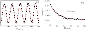
By using the bridge technique of pre-exposure, we fabricated the 3D transmon qubit[22] based on a sapphire substrate. Its Rabi oscillation and relaxation time (T1 ∼ 20 μs) (Fig.
We have investigated the pre-exposure technique using a 30-keV e-beam writer to fabricate Al/AlOx/Al Josephson junctions. Both bridge and bridge-free techniques are studied. Similar results, comparable with those achieved using the 100-keV e-beam writer, are obtained. The undercut of the bilayer resist can be well controlled. High-quality junctions with the area ranging from 0.04 μm2 to 10 μm2 are fabricated. Our results indicate that the 30 keV e-beam writer can be an economic choice for the pre-exposure technique in the superconducting qubit fabrication.
| 1 | |
| 2 | |
| 3 | |
| 4 | |
| 5 | |
| 6 | |
| 7 | |
| 8 | |
| 9 | |
| 10 | |
| 11 | |
| 12 | |
| 13 | |
| 14 | |
| 15 | |
| 16 | |
| 17 | |
| 18 | |
| 19 | |
| 20 | |
| 21 | |
| 22 |


