† Corresponding author. E-mail:
Project supported by the National High Technology Research and Development Program of China (Grant No. SS2015AA010601), the National Natural Science Foundation of China (Grant Nos. 61176091 and 61306129), and the Opening Project of Key Laboratory of Microelectronics Devices & Integrated Technology, Institute of MicroElectronics of Chinese Academy of Sciences.
High-k metal gate stacks are being used to suppress the gate leakage due to tunneling for sub-45 nm technology nodes. The reliability of thin dielectric films becomes a limitation to device manufacturing, especially to the breakdown characteristic. In this work, a breakdown simulator based on a percolation model and the kinetic Monte Carlo method is set up, and the intrinsic relation between time to breakdown and trap generation rate R is studied by TDDB simulation. It is found that all degradation factors, such as trap generation rate time exponent m, Weibull slope β and percolation factor s, each could be expressed as a function of trap density time exponent α. Based on the percolation relation and power law lifetime projection, a temperature related trap generation model is proposed. The validity of this model is confirmed by comparing with experiment results. For other device and material conditions, the percolation relation provides a new way to study the relationship between trap generation and lifetime projection.
High-k metal gate stacks are being used to suppress the gate leakage due to tunneling for sub-45 nm technology nodes.[1–3] Multi-layer gate dielectric of the high-k/interfacial layer (HK/IL) brings not only promising performance but also reliability challenges. Especially for sub-1-nm equivalent oxide thickness (EOT) metal oxide semiconductor (MOS) devices, the reliability of thin dielectric film becomes a limitation to device manufacturing.[4–6]
For thin dielectric, the breakdown characteristic is no longer the same as classical electric field (E-field) driven phenomenon. A number of studies suggest that the trap generation in oxide is the main cause for final breakdown.[7–9] The breakdown events are related to the trap generation process and percolation path formation. For a lifetime projection model, a universal power law model is obtained over wide ranges of EOT and stress voltage.[10,11] It is evident that different models yield drastically different lifetime results in affecting the specification supply voltage.
The percolation theory has proved that the distribution of breakdown events is an intrinsic mechanism.[8] By using Monte Carlo (MC) simulation, the area scaling law and Weibull distribution are obtained, and the decrease of Weibull slope with reducing oxide thickness is well explained. Furthermore, with an application of the kinetic Monte Carlo (kMC) method, bimodal Weibull distribution of TDDB is explained as different trap generation rates in high-k and interfacial layer.[9]
In this work, based on the percolation model and the kinetic Monte Carlo (kMC) method, a simulator of the breakdown process is set up. The intrinsic relation between time to breakdown and trap generation rate R is studied by simulations. The degradation factors each are written as a function of trap density time exponent α. By combining the percolation relation with power law lifetime projection, a temperature related trap generation model is proposed to study the dielectric degradation. It is found that the generated trap is thermally activated, with the activation energy being about 0.11 eV. For different device and material conditions, the trap generation process could also be connected with the breakdown characteristic by the percolation relation.
MOS capacitors are fabricated as follows. Firstly, Si wafer with a resistivity of 2 Ω ∼ 4 Ω for n-type is cleaned by diluted buffered oxide etch solution. Then the interfacial layer is formed by ozone oxidation. The HfO2 layer is deposited by atom layer deposition (ALD) with about 2.4-nm-thick used as the high-k dielectric. Continuously, post annealing at 450 °C is treated. Then a 2-nm-thick TiN and a 1-nm-thick TaN layer are formed by ALD, and a 3-nm-thick TiN layer by chemical vapor deposition (CVD). Finally, 75-nm-thick W layer are deposited as gate electrode.
All electric measurements are performed by an Agilent 4155B and 4294A. The temperature in measurement ranges from 25 °C to 125 °C. MOS capacitors are stressed in the accumulation area for constant voltage stress (CVS) and ramp voltage stress (RVS). The areas under test are all 100 μm2. The EOT of gate stacks is about 1.07 nm and the physical thickness of HfO2 is about 2.4 nm. An abrupt increase of gate current is used as the failure criterion and the current after breakdown is about 2 mA.
Percolation model simulations are conducted based on the kMC method on a three-dimensional (3D) cubic grid. The dielectric is divided into 100×100 cells in the plane of the substrate and 3-to-6 layers of dielectric. Thus, the edge effect is negligible. For each set of simulations, 64-1000 breakdown events are recorded to fit the experiment results. The flowchart of the simulation is shown in Fig.
In each simulated step, a new trap is generated in a random site and time evolves in a random increment influenced by the time dependent trap generation rate. When a percolation path connecting two interfaces, the breakdown event is recorded.
In this work, the trap density time exponent α = 0.38 is used according to Ref. [9]. Then, 6 of the total dielectric layers could be used in simulation due to a constant experiment Weibull slope of about 2.3. Then the gate dielectric is treated as a 4-layer high-k + 2 layer IL and the trap effect distance a0 = 6 Å. The trap generation rates of high-k and IL are treated as the same value due to the single Weibull distribution in this work. The Weibull distribution of simulation results is normalized based on the Poisson area scaling law to an experiment test area.
The trap generation rate R in each cell is defined as follows:

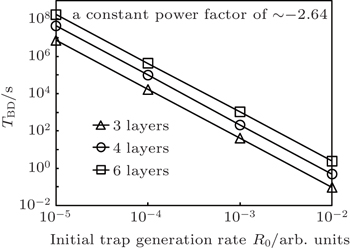
Based on the above trap generation rate, the relation between TBD (time to breakdown) and initial trap generation rate R0 could be studied by simulation. The trap generation rate time exponent m is set to be −0.62 according to trap density time exponent α.
The simulation results by varying initial trap generation rate are shown in Fig.

Based on the above results, it is concluded that s is independent of dielectric thickness and only dependent on degradation factor m. It is the result of an intrinsic characteristic of percolation theory and independent of lifetime projection and statistics. Thus, s could be regarded as a degradation factor. The percolation factor is also a useful parameter to connect percolation simulation and lifetime projection.
Here, a detailed study is given to describe the relation of degradation factors. All degradation parameters are useful to study the dielectric degradation process, including trap density time exponent α, trap generation rate time exponent m, Weibull slope β and percolation factor s.
Firstly, α is the time exponent factor of trap density, as shown below


Based on the above discussion, α and m are physical parameters related to the trap generation process during stress tests. The other two parameters s and β are simulation factors in the percolation model simulation.
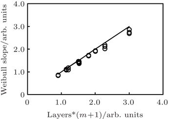
The Weibull slope β is one of the simulation degradation factors. The value of Weibull slope describes the spreading characteristic of TBD distribution. The relation of β is obtained from simulation results (Fig.

Finally, the percolation factor s in the percolation relation is also studied in the relation with α. An intrinsic relation between s and α is obtained below and shown in Fig.

As a conclusion, with percolation model simulation, all degradation factors could be expressed as functions of trap density time exponent α. All these parameters are related to the trap generation process and dielectric breakdown. These parameters are useful in reliability assessment and lifetime projection.
Temperature related model is significant for the in-depth understanding of the trap generation process. In TDDB measurements, stress voltages are from 2.7 V to 3.2 V and temperatures are set to be 25 °C, 60 °C, 90 °C, and 125 °C, respectively. Under each measurement condition, 11–20 devices are tested for truncated statistic analysis and the Weibull distributions for test results are shown in Fig.
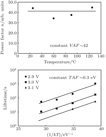
Based on TBD extracted from the above TDDB results, a temperature related power law model is proposed for lifetime projection. It could be written as

Based on the above lifetime projection model and percolation relation, combining Eqs. (

This model indicates that the trap generation is a thermal activation process and the activation energy of the generated trap is about 0.11 eV in this paper. The activation energy and voltage power law factor of the generated trap could be obtained from VAF and TAF in the lifetime projection and percolation factor s.
From the above results, the trap generation model is determined by the lifetime projection and percolation relation. For other conditions, lifetime projection models are different, especially for temperature dependence.[16–18] Thus, for different materials and devices, the trap generation model should be corrected with the lifetime projection model and percolation relation. The trap activation energy Ea could be obtained from the TAF and percolation factor s for different materials.
In this work, a temperature and voltage dependent trap generation model is proposed. It is useful for TDDB simulation and lifetime projection in reliability assessment. A simulator of the breakdown process is set up based on the percolation model and the kMC method. The intrinsic relation between TBD and initial trap generation rate R0 is obtained from simulation results. The power exponent s is defined as the percolation factor due to the intrinsic percolation relation. Four degradation related factors could be unified as functions of trap density time exponent α. By combining the percolation relation with the power law model, the temperature and voltage dependent trap generation model is obtained. It is found that the trap generation process is a thermal activation process, with the activation energy being 0.11 eV. The power exponent and activation energy of trap generation are correlated with the VAF, TAF in the power law model and percolation factor s. A good correlation with experimental results confirms the validity of this model. This model is applicable in percolation model simulation and provides a new way to study the trap generation process and lifetime projection. For other device and material conditions, the trap generation process could be related to the lifetime projection model through the percolation relation.
| 1 | |
| 2 | |
| 3 | |
| 4 | |
| 5 | |
| 6 | |
| 7 | |
| 8 | |
| 9 | |
| 10 | |
| 11 | |
| 12 | |
| 13 | |
| 14 | |
| 15 | |
| 16 | |
| 17 | |
| 18 |


