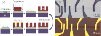
1. IntroductionGraphene, a single layer of carbon atoms, with a honeycomb structure, has attracted wide attention among scientists since 2004 due to its unique properties. Its application covers a wide range of areas, including energy storage,[1] flexible touch screen,[2] radio frequency (RF) devices,[3] supercapacitors,[4] and biosensors.[5] Owing to graphene’s extremely high electron mobility, the graphene field effect transistor (GFET) has been proposed as a candidate electronic device in the post silicon era.[6] However, due to the lack of bandgap in graphene, the GFET cannot be turned off completely. Hence, much attention has recently shifted to the use of graphene in RF transistors, where the OFF-current is less critical than that in a digital circuit. One of the figures of merit of GFET in RF domain is the cutoff frequency (fT) and the previous studies have shown that the cutoff frequency can be significantly improved by reducing the contact resistance.[7–11] Hence, various teams have introduced different methods to reduce the contact resistance. Low power O2 plasma treatment[12] and UV/ozone treatment[13] are employed to eliminate the residues at the contact area and create a certain degree of defects on graphene for a better contact. But the demanding control of the experimental conditions limits its popularity and validity since an overtime treatment might increase the contact resistance instead of improving it and the treatment time and conditions could vary from lab to lab. Annealing in vacuum or H2/Ar atmosphere above 300 °C can also eliminate the resist residues on graphene[14] but with a drawback of deteriorating the properties of graphene in the channel by inducing increased coupling between graphene and the substrate.[14–16] Other methods like the current annealing,[17] electrostatic force cleaning,[18] and mechanical force cleaning via atomic force microscopy (AFM)[19] are all unsuitable for large scale fabrication. Using a metal as a protective layer is another alternative to prevent the contamination of residues, but the results are not good enough with the contact resistance ranging 200–500 Ω·μm[7] and 500 Ω·μm,[20] and the protective metal deposited on the channel can create defects in graphene during the metal etching process.[21] Using nickel-catalyzed etching[22] to form edge contacts and H-plasma anisotropic etching to form multilayer contacts[23] are methods both aimed at treating the contact area and the channel differently. But these works focused on the exfoliated sample, and samples from chemical vapor deposition (CVD) method need further investigation. So herein, we provide a simple method to reduce the contact resistance by depositing a thin layer of aluminum (5 nm) on the contact area after development and etching it away while keeping the graphene in the channel intact. Aluminum is rapidly etched in an alkaline solution, which contains tetramethylammonium hydroxide (TMAH). The fast etching process functions as a cleaning process and modifies the surface of graphene by alleviating the doping from the photoresist in the contact area. After this treatment, we deposit the final contact metal Pd/Au followed by a lift-off process. Palladium is chosen as the contact metal due to its good wettability[24] on graphene. Due to the protection of photoresist on the graphene channel, the trade-off between decreasing the contact resistance and deteriorating the property of the GFET such as mobility on the channel will not happen compared to the other methods.
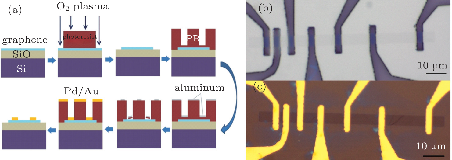
3. Results and discussionThe optical image after etching the aluminum layer is shown in Fig. 1(b). After the lift-off process of Pd/Au, the ultimate TLM structure is shown in Fig. 1(c). These images show that the aluminum etching process does not damage the pattern after treating the contact area. The effect of depositing metal and etching it away on graphene could be explained as a cleaning procedure proposed by Joiner et al.[25] The aluminum in this procedure behaves like a sticky tape which is similar to the demonstration of Dimiev et al.[26] Aluminum is etched quickly in the solution containing TMAH which shows a strong alkaline property.[7,27] Moreover, we think that the treatment might introduce some edge contacts by creating some defects[21] in the contact area, which is helpful to reduce the contact resistance,[28] but this needs further investigation.
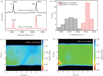
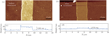
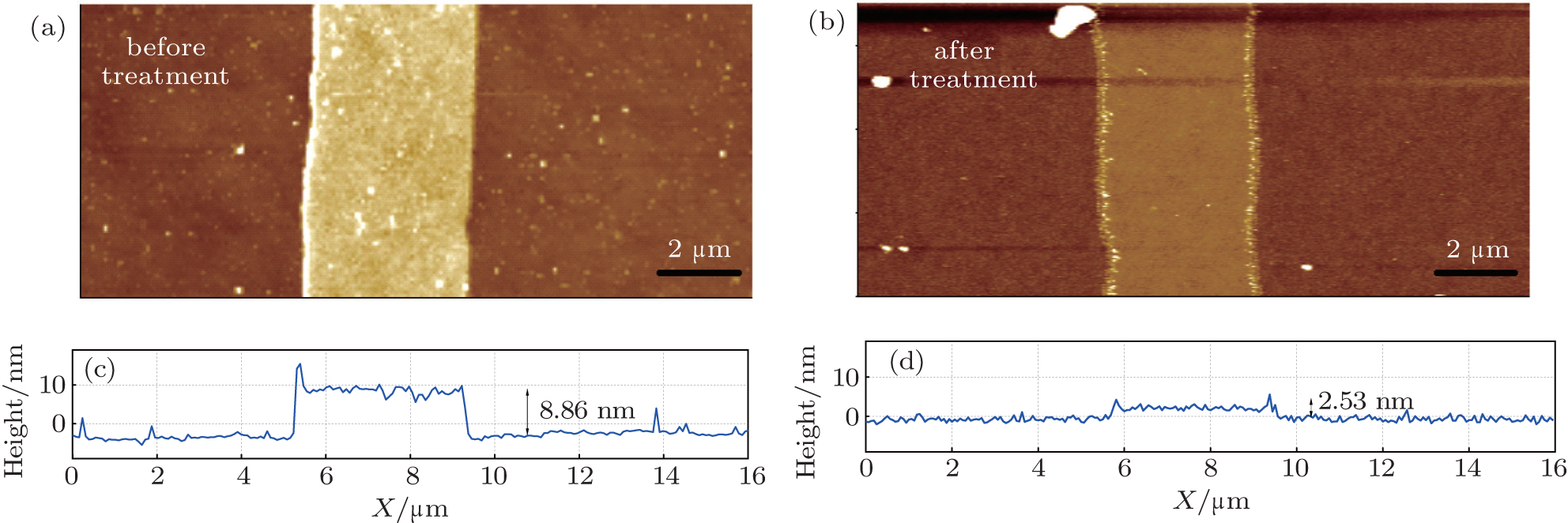
To verify the cleaning effect on graphene, Raman spectroscopy was performed before and after the aluminum treatment, the results are shown in Fig. 2. The “before treatment” results are for the graphene sample gone through the whole processing steps without the deposition of aluminum, while the “after treatment” results are for the sample with a 5 nm-thin layer of aluminum deposited on graphene and then etched away. In order to illustrate the effectiveness of the treatment, a Raman mapping of 8 × 6 points with a step of 1 μm on a graphene strip was also conducted. A comparison of the Raman results before and after the treatment is shown in Fig. 2(a). Before the treatment, the high intensity of the G band and its blue shift to 1594 cm−1 are indications of high doping in graphene.[29] After the treatment, the G band position moves back to 1587 cm−1 and the G band intensity decreases which is shown as an increase of the intensity ratio (I(2D)/I(G)) from 1.10 to 1.86. The Raman mapping results of the intensity ratio (I(2D)/I(G)) and the statistic results of the G band position are shown in Figs. 2(b)–2(d), respectively, which show a similar trend to the results in Fig. 2(a). From the Raman spectra, we find that the treatment has mitigated the doping of graphene, which could be attributed to the removal of organic residues such as PMMA and other photoresists.[12,13] The removal of the residues could also be verified by the AFM results, which are shown in Fig. 3. A graphene strip of 4 μm width was measured via AFM before and after the treatment. The height of graphene is reduced from nearly 8.86 nm to 2.53 nm after the treatment, indicating a cleaning effect through the treatment, which is consistent with the discussion of the Raman results.
Since we focused on reducing the contact resistance, the TLM structure was fabricated to compare the results. In a TLM array, the total resistance between two metal pads consists of three components[20]

where
Rm and
Rc are the resistances from the contact metal and the metal/graphene interface, and
Rgr is the intrinsic resistance of graphene which increase linearly with the channel length. The resistance of a single contact would be
Rm +
Rc. However, in most cases, the resistivity of the metal is so low that
Rc ≫
Rm, and
Rm can often be ignored. So when plotting the relationship between the total resistance and the channel length, the intercept on the resistance axis equals twice the value of the contact resistance. Since different channel width will result in different extracted contact resistance, for the comparison between different research teams, the contact resistivity is used instead. In the TLM structure, the relation between the contact resistivity (
ρc) of the graphene/metal interface and the contact resistance (
Rc) can be written as
[13,30]

where
Lc and
W are the length and width of the electrode contact, and
LT is the transfer length defined by the distance at which the current drops to 1/e from the contact edge. In most cases,
LT ranges between tens and several hundred nanometers,
[8,30] and
Lc ≫
LT, so
Rc ≈
ρc/(
WLT). Also, because
LT is so small, it is more convenient to use
Rc·
W with the unit of Ω·μm to compare the findings.
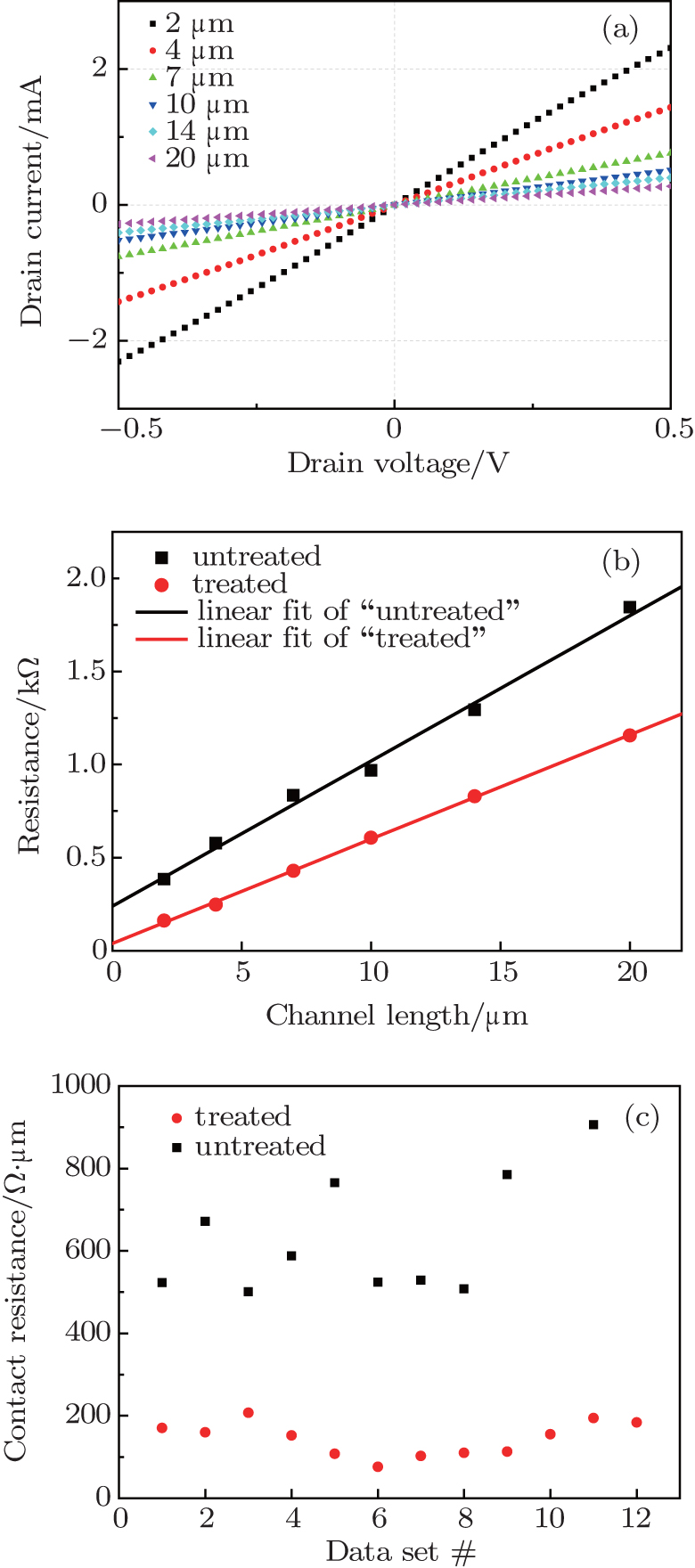
We design the TLM structure with the width of 5 μm and the length of L1 = 2 μm, L2 = 4 μm, L3 = 7 μm, L4 = 10 μm, L5 = 14 μm, L6 = 20 μm. The electrode pad length (Lc = 3 μm) is much larger than the transfer length. Figure 4(a) shows the dependence of the I–V curve on the channel length. The I–V characteristics are linear over a large applied voltage range, indicating that the contacts are ohmic. The total resistance was extracted from the I–V curve and its dependence on the channel length is shown in Fig. 4(b). The aluminum cleaned set is shown as “treated” while “untreated” represents the set which comes from the same graphene material and has gone through the same fabrication process except for the aluminum treatment procedure. Due to the larger absolute errors in extracting the contacting resistance when the gate bias is around VDirac,[8] which is indicated as the minimum conductance point, we choose to compare the treated and untreated samples at the same back-gate bias of −40 V. According to the data, the graphene devices without the treatment show a larger contact resistance around 597 Ω·μm with a larger standard deviation due to the non-uniformly distributed photoresidues. On the other hand, the devices gone through aluminum cleaning have a smaller contact resistance of 98.73 Ω·μm and a smaller standard deviation. Several devices were tested and a distribution of sub 200 Ω·μm for the treated devices is shown in Fig. 4(c). With the smallest value reaching to 75 Ω·μm, the results are better than the previous reported ones.[7,20]
We have to mention that this treatment only influences the contact area, and the channel area is protected by photoresist. So compared to the method of depositing an aluminum layer onto the whole graphene surface shown by Allen Hsu et al.,[7] this method will not deteriorate the device’s other properties such as motility as a trade-off.[7] To extract the mobility of the graphene devices, the transfer characteristic curve was measured by applying a gate voltage ranging from −40 V to 80 V to the back-gate substrate while applying a drain–source voltage of 5 mV. The Rtot–Vg curve shown in Fig. 5(a) was fitted by the model proposed by Kim.[31] The extracted hole mobility is 814.42 cm2/V·s and the extracted electron mobility is 670.18 cm2/V·s. Although the fitting is good, there are still some discrepancies on the hole branch, we attribute this to the imprecise value of gate capacitance[32] and the mobility variation near the Dirac point and away from the Dirac point.[32,33] To testify that there is no degradation using this method, we compare the mobility distributions of the treated and untreated samples in Fig. 5(b). The treated and untreated samples both have a mobility in the range of 400–1000 cm2/V·s. There is a slight increase for the treated samples and we attribute this enhancement to the decrease of the intrinsic carrier concentration induced by charged impurities.[34] This result meets the expectations: decreasing the contact resistance while preserving the mobility of the channel.


 , Wang Shao-qing, Zhang Da-yong, Shi Jing-yuan, Peng Song-ang, Wang Xuan-yun]