Depositing aluminum as sacrificial metal to reduce metal–graphene contact resistance
Mao Da-cheng, Jin Zhi†,  , Wang Shao-qing, Zhang Da-yong, Shi Jing-yuan, Peng Song-ang, Wang Xuan-yun
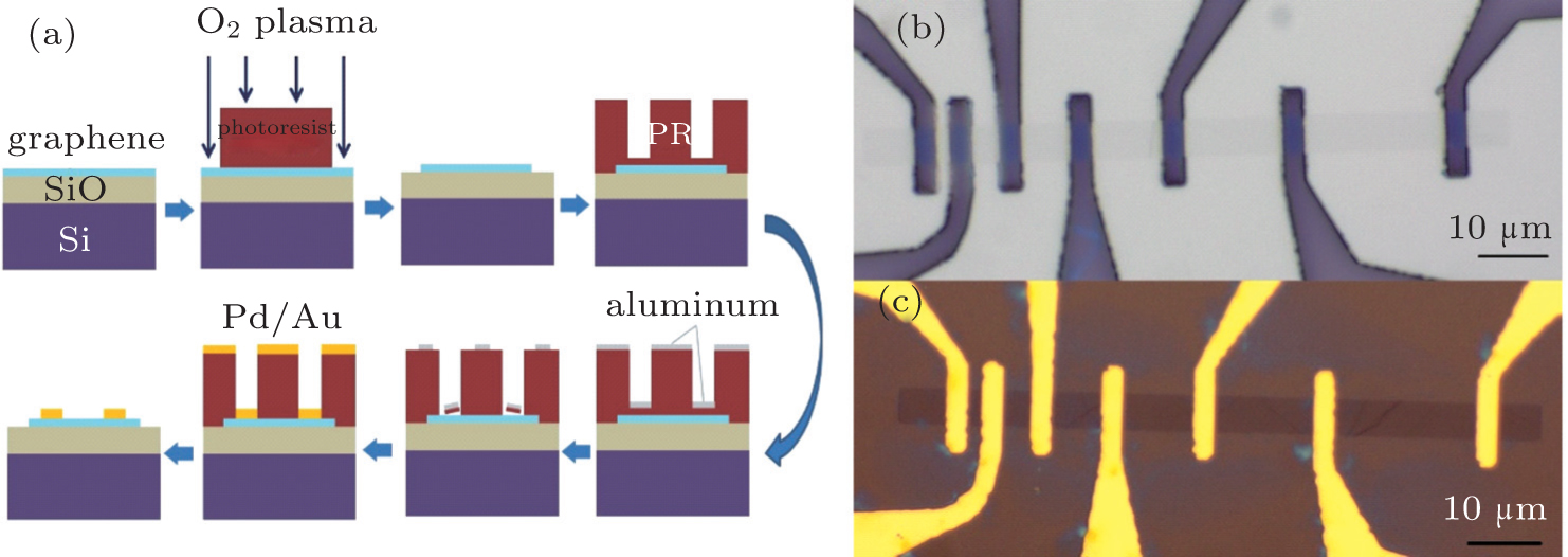
, Wang Shao-qing, Zhang Da-yong, Shi Jing-yuan, Peng Song-ang, Wang Xuan-yun (a) Schematic illustration of the fabrication process of graphene FET devices. (b) Optical image after etching the aluminum layer. (c) The TLM structure after depositing the final metal pad.