† Corresponding author. E-mail:
Project supported by the National Natural Science Foundation of China (Grant Nos. 61176092 and 61474094), the National Basic Research Program of China (Grant Nos. 2012CB933503 and 2013CB632103), and the National Natural Science Foundation of China–National Research Foundation of Korea Joint Research Project (Grant No. 11311140251).
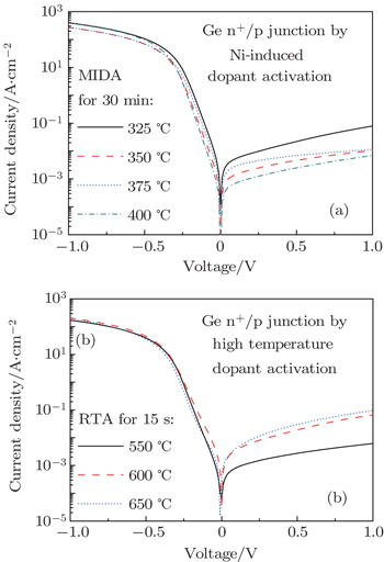
High-performance Ge n+/p junctions were fabricated at a low formation temperature from 325 °C to 400 °C with a metal(nickel)-induced dopant activation technique. The obtained NiGe electroded Ge n+/p junction has a rectification ratio of 5.6× 10⁴ and a forward current of 387 A/cm2 at −1 V bias. The Ni-based metal-induced dopant activation technique is expected to meet the requirement of the shallow junction of Ge MOSFET.
Germanium (Ge) has been considered as the best candidate to replace the traditional Si to fabricate next-generation metal–oxide–semiconductor field-effect transistors (MOSFET) because of its high carrier mobilities. However, the low activation level and fast diffusion of the implanted phosphorus (P) in Ge hinder the formation of high-quality shallow Ge n+/p junctions.[1] As a result, Ge n-MOSFET is confronted by more process challenges as compared to its p-MOSFET counterpart.[2]
To fully activate the dopant atoms as well as to control the dopant redistribution depth, a metal-induced dopant activation (MIDA) technique has aroused much research interest recently. Park et al. studied dopant activation of α-Ge by films of various metals including Pd, Cu, Au, Co, and Ni (Nickel).[3] According to his results, Ni was not considered as a good choice to activate the implanted P dopant atoms because Ni itself acts as acceptor-like traps in Ge. Later, Nishimura et al. fabricated Ge n+/p junctions by Ni/NiGe induced dopant activation.[4] However, the rectification ratio of the junctions is only about 103, which is one order of magnitude lower than the junctions formed by the Pt[5] and Co[6] induced dopant activation.
Ni and Ni germanide (NiGe) have been widely used as the source/drain contact in Ge MOSFET. When the Ni film was annealed on the implanted Ge to facilitate MIDA, NiGe simultaneous formed even at temperatures as low as 300 °C. NiGe film has a resistivity of 22 μΩ·cm which is the lowest among all metal germanides as far as we know.[7] On the other hand, as the top Ge is consumed during the NiGe formation, a snow-plow effect[8] may accumulate dopant atoms at the germanide/Ge interface which is favored for low-contact-resistivity shallow junction fabrication.
In this work, we demonstrate high performance Ge n+/p junctions formed by low temperature annealing from 325 °C to 400 °C with Ni-induced dopant activation. A rectification ratio of 5.6× 10⁴ and high forward current of 387 A/cm2 were obtained.
P-type Ge(001) wafer with a resistivity of 0.06 Ω·cm and undoped Ge(100) wafer with a resistivity of 50 Ω·cm were cleaned by acetone, ethanol, HCl solution, and finally dipped by HF solution. After being covered with 15-nm-thick SiO2 by plasma-enhanced chemical vapor deposition, these wafers were implanted by P+ ions with the acceleration voltage of 30 keV and the dose of 1× 1015 cm−2. After the top SiO2 buffer layer was stripped, 25-nm-thick Ni was deposited in an e-beam evaporation system. The Ni film was then patterned by optical lithography and HCl solution (HCl:H2O = 1:1) etching. Using the patterned photoresist as a shield, ICP etching continuously etched the exposed Ge to form circular junction plateaus with a diameter of 160 μm. The Ge etching depth was set 800 nm to make sure all the exposed Ge implantation layers were totally removed. The photoresist was then stripped and the samples execute thermal annealing at temperatures from 325 °C to 400 °C in nitrogen atmosphere for 30 min to perform MIDA. NiGe layer formed as well. 300 nm of Al was finally deposited on the back side of the samples for ohmic contact.
As a comparison, n+/p junctions by conventional rapid thermal annealing (RTA) were also prepared. The cleaning, implantation, and Ni deposition were the same as above. However, before SiO2 stripping and Ni deposition, the wafers were pre-annealed at the 550–650 °C temperature range for 15 s to replace the MIDA annealing. A 400 °C/30 s annealing was used to form NiGe electrode.
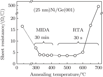
In a conventional Ge n+/p junction process, the implanted P+ atoms require an RTA annealing over 500 °C to be fully activated. Figure
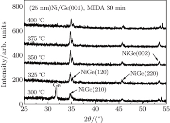
As observed by many studies, the Ge surface was severely damaged and even transformed into α-Ge after high-dose ion implantation. High temperature annealing is required to recrystallize the top amorphous layer as well as to activate the dopants. The α-Ge has been reported to be fully crystallized at above 450 °C.[7] However, in MIDA, the diffused metal atoms in the implanted Ge weaken the bonds in Ge and lower the temperature for homogeneous nuclei formation. As the nuclei grew into crystals, the dopant atoms are also rearranged and activated subsequently. To find a suitable MIDA temperature for NiGe electroded n+/p junction preparation, the (25 nm) Ni was annealed on undoped Ge to check the resistance and the material phase. Figures
Current–voltage (I–V) characteristics were measured on the MIDA Ge n+/p junctions. Figure
 | Fig. 3. X-ray diffraction patterns of the (25 nm)Ni/Ge(001) after annealing for 30 min at various temperatures. |
We also tried P+ implantation through thick SiO2 windows to fabricate MIDA Ge n+/p junctions. However, the measured IV curves show a rectification ratio only about 102. As is known, there are a large number of surface states when Ge directly contacts with SiO2, which contributed to the leakage path across the edge of the n+/p junctions. Hence, a good surface passivation method could be important to reduce the leakage current at negative bias and increase the rectification ratio of the Ge n+/p junctions.
| Table 1. Rectification ratios and extracted ideality factors of Ge n+/p junctions fabricated by various dopant activation methods. . |
The corresponding P, Ni, Ge elemental distributions were measured by secondary ion mass spectroscopy (SIMS) as shown in Fig.
The Ni film was transformed into NiGe phase after annealing. Figure
The snow-plow effect was not observed because the Ni film in our experiment is not thick enough. The P dopants distribute across the NiGe/Ge(100) interface and within the shallow surface of the Ge substrate, but not yet reaching the outside surface of the NiGe layer. By tuning the process parameters such as reducing the P+ implantation energy or using a thicker Ni layer, the P distribution throughout the NiGe layer and the n+/p junction could be modulated. An optimized implantation/germanidation process combined with the MIDA annealing can be beneficial to forming a shallow junction which is required by the scaling MOSFETs.
In summary, using Ni as the metal layer for MIDA of the implanted P dopant in Ge, a high rectification ratio of 5.6× 10⁴ and a forward current of 387 A/cm2 at −1 V bias is obtained for Ge n+/p junction. The high rectification ratio is ascribed to the suppression of the surface leakage and limited diffusion of the Ni in Ge. SIMS shows that the P redistribution in the MIDA junctions is less significant that the junctions activated at high temperatures. The MIDA Ge n+/p junction may find its application in novel Ge n-MOSFET.
| 1 | |
| 2 | |
| 3 | |
| 4 | |
| 5 | |
| 6 | |
| 7 | |
| 8 | |
| 9 |


