High-performance germanium n+/p junction by nickel-induced dopant activation of implanted phosphorus at low temperature
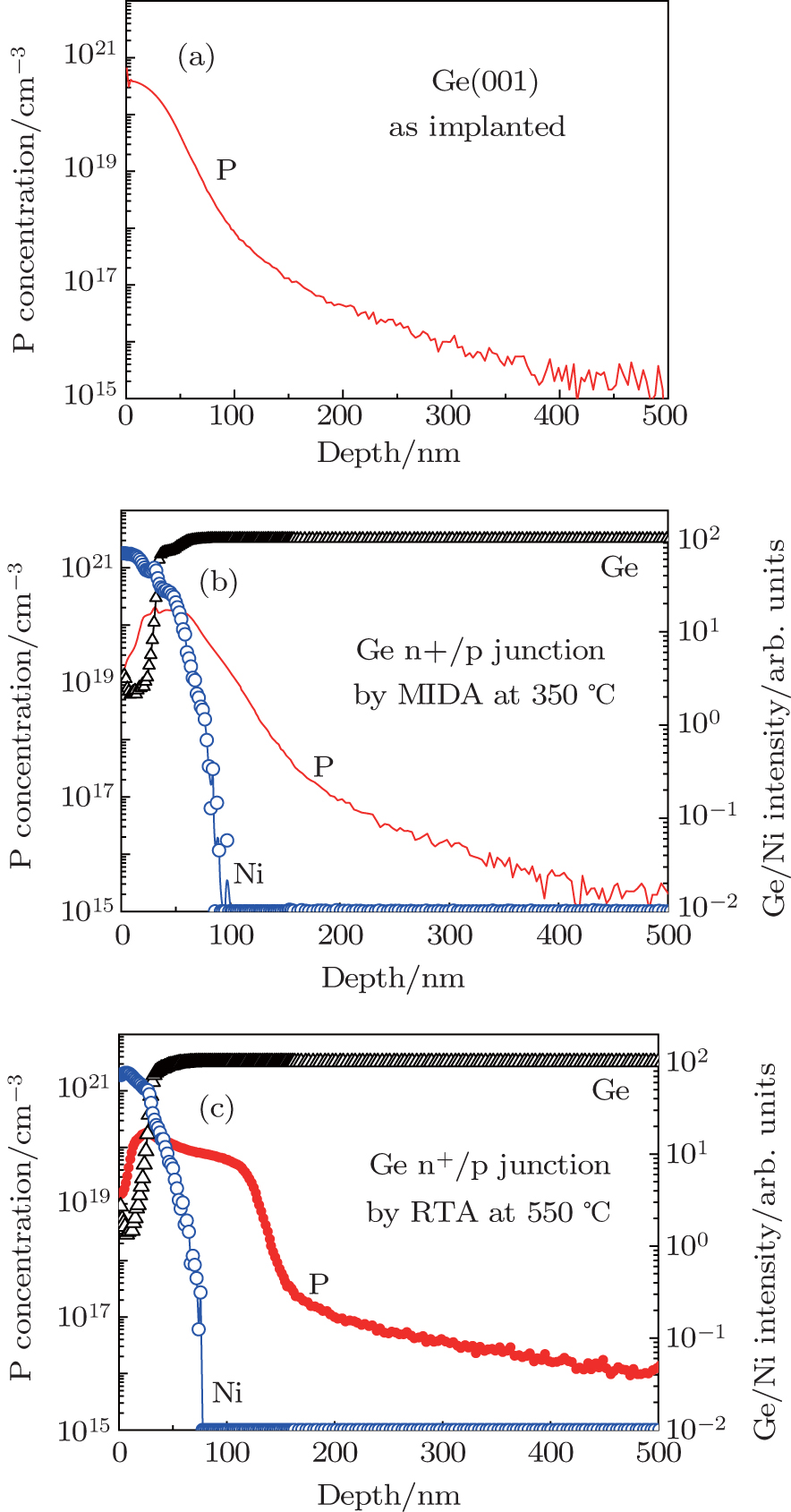
P, Ni, and Ge distribution profiles measured by SIMS for (a) Ge(100) substrate after P+ implantation, (b) Ge n+/p junction after MIDA annealing at 350 °C for 30 min, and (c) Ge n+/p junction after RTA activation annealing at 550 °C for 15 s.

