† Corresponding author. E-mail:
Project supported by the National Basic Research Program of China (Grant No. 2014CB339900) and the Open Fund of Key Laboratory of Complex Electromagnetic Environment Science and Technology, China Academy of Engineering Physics (Grant No. 2015-0214.XY.K).
In this paper, we present the damage effect and mechanism of high power microwave (HPM) on AlGaAs/GaAs pseudomorphic high-electron-mobility transistor (pHEMT) of low-noise amplifier (LNA). A detailed investigation is carried out by simulation and experiment study. A two-dimensional electro-thermal model of the typical GaAs pHEMT induced by HPM is established in this paper. The simulation result reveals that avalanche breakdown, intrinsic excitation, and thermal breakdown all contribute to damage process. Heat accumulation occurs during the positive half cycle and the cylinder under the gate near the source side is most susceptible to burn-out. Experiment is carried out by injecting high power microwave into GaAs pHEMT LNA samples. It is found that the damage to LNA is because of the burn-out at first stage pHEMT. The interiors of the damaged samples are observed by scanning electron microscopy (SEM) and energy dispersive spectrometer (EDS). Experimental results accord well with the simulation of our model.
With the rapid development of high power microwave (HPM) source generation technology, growing attention has been paid to the threat posed by intentional electromagnetic interference (IEMI).[1–7] Such an HPM induced by IEMI could couple into the interior electronics of a system through two generic ways, i.e., front-door coupling and the back-door coupling, which could disrupt or destroy a device. The effect of man-made electromagnetic interferences on electronic systems is an ongoing and wide research topic.[7–10]
The malfunction/destruction failure rate (M/D FR) was measured to investigate the susceptibility of LNA due to front-door coupling under narrow-band high power electromagnetic wave.[11] Experimental measurements of susceptibility of electronics to HPM and UWB irradiation with repetition rate signals were presented in Ref. [12]. The injecting method was adopted to study the microwave vulnerability effect of integrated circuits (ICs) in Ref. [10]. Experimental results from the radiation method of microwave pulses effect in L band on personal computer (PC) were presented in Ref. [13]. The HPM induced latch-up effect on complementary metal–oxide semiconductors (CMOS) have been studied in Ref. [14]. A theoretical study of the EMP damage mechanism and the susceptibility trend of pulse parameter-dependent are discussed in Refs. [15]–[18].
As for an electric system, LNA is a key element in RF front-end of the wireless receiver, which is generally the most sensitive section at the same time. Owing to the potential application to high breakdown voltage, low on-resistance and high frequency, AlGaAs/GaAs pseudomorphic high-electron-mobility transistor (pHEMT) gradually serves as the core element in LNA. In previous studies, the burnout characteristics of GaAs MESFET were studied in Refs. [19] and [20]. In Ref. [21], four types of defects on damaged GaAs HEMT MMIC were analyzed. The degradation effect of GaAs pHEMT induced by HPM was discussed in Ref. [22]. The burnout properties of the GaAs pHEMT was analyzed in Ref. [23]. However, the study mentioned above placed emphasis on the experimental study, theoretical research was not sufficient, it needs further studying.
This paper focuses on the damage effect of pHEMT induced by front-door coupling HPM. Firstly, a two-dimensional (2D) electro–thermal model of a typical pHEMT is established with the device simulator Sentaurus-TCAD. Secondly, the damage process and physical mechanism are simulated. The variations of device internal electric field, the current density and the temperature distributions with time are analyzed. Finally, an experiment is carried out by injecting HPM into LNA, and the characteristics of damage morphology are analyzed by using scanning electron microscopy (SEM). The energy dispersive spectrometer (EDS) is used to analyze elemental composition at the location of burn-out.
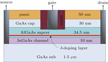
Figure
To investigate the damage effect, the advanced mixed mode device and circuit on GaAs pHEMTs is simulated by using Sentaurus-TCAD. The presence of high current and high voltage causes a huge joule heat within the device, which may lead to a sharp rise in temperature during the injection of HPM. Hence the nonuniform temperature distribution and heat diffusion are major concerns. For crystalline materials, they need many thermo-related parameters to describe the thermodynamic behavior among which lattice thermal conductivity and specific heat are the two most important parameters. Both of them are susceptible to temperature variation, hence they cannot be regarded as constant any more when temperature increases. The fitting curve (line) used in the simulation on the basis of the experiment data[24,25] (scatter plot) is shown in Fig.


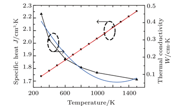 | Fig. 2. Variation trends of lattice thermal conductivity and specific heat with lattice temperature increasing. |
Additionally, there are a number of physical models used in simulation such as mobility degradation in high electric field, avalanche generation effect and self-heating effect. Since the drift-diffusion approach often overestimates the ionization generation rate, the hydrodynamic model is employed to provide a better accuracy. For the numerical expression of the physical model mentioned above, it can be seen in Ref. [27]. Here, we will not go into details of them.
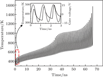
For the transistor shown in Fig.
It can be seen that the maximum temperature within device keeps increasing under the action of microwave, and finally rises up to the 1511 K (GaAs melting point) at the 66th period. The variation of temperature in the first three periods is illustrated in the inset. It indicates that the temperature behaves as periodical increasing–decreasing–increasing. It increases during positive half cycle and then decreases during negative half cycle. To explain this phenomenon, the current density and electric field at 0.25 ns and 0.75 ns are shown in Fig.
According to Fig.
During the negative cycle, the Schottky junction is reverse-biased. Therefore, the current density is extremely low (Fig.
It is also indicated that the overall temperature increase shows that the temperature sudden rises twice, in which the first time rising is at 32 ns and the second time rising is at 64 ns. A detailed investigation of the damage process is performed by analyzing the variations of the electric field, the current density and the temperature in the device with time.
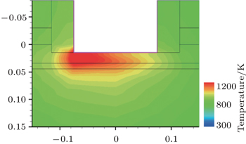
Figure
Figure
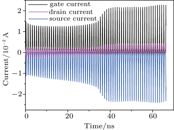 | Fig. 6. Variations of of current density at gate (black), source (blue), and drain (red) electrode with time. |
Figure
In order to study the electric field distributions during the damage process, electric field at four typical moments: 0.25 ns, 35.25 ns, 50.25 ns, and 66 ns, are selected. Figure
From the above discussion, it follows that under the joint action of electric field and current density, the increase of current is the leading factor for the first sudden rise of temperature which is induced by intrinsic excitation. With the heat accumulation, a positive feedback is formed between the heat accumulation and the thermal breakdown when the temperature is equal to or greater than 1200 K. It will cause the electric field to increase immediately, and it will also causes the temperature to increase till burn-out. Figure
In order to verify the previous explanations, experiment is performed by directly injecting microwave power into LNA sample which consists of two GaAs pHEMTs: one is the first stage (numbered as 11#) and the other is the second stage (numbered as 1-2#). The injected HPM signals are continuous waves with high density power. The noise figure of LNA deteriorating by 20 dB is determined as a damage criterion.[29]
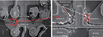
The DC characteristic is tested on two pHEMT samples. Sample 1-1# shows short character, and the sample 1-2# shows the junction feature. It can be inferred that the damage of the first stage is responsible for the failure of LNA. Further research about the HPM damage effect is carried out by using SEM to observe the interior of the sample 1-1#.
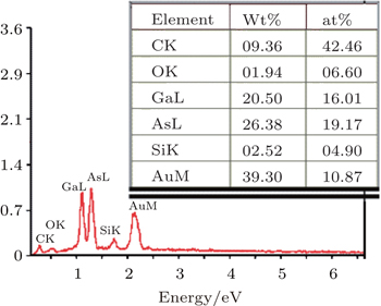
From the interior features of sample #1-1 characterized by SEM, it can be seen that, the gate-to-source channel is obviously overheating and burned and one or more molten globules and pits emerge between the source and gate contact (see Fig.
In this paper we investigate the damage effect of HPM on a two-stage LNA which consists of GaAs pHEMTs. A typical δ -doped pHEMT induced by the pulsed microwaves is established with the device simulator Sentaurus-TCAD by considering the mobility degradation in high electric field, avalanche generation effect and self-heating effect. According to the analyses of the variations of device internal distributions of the electric field, the current density and the temperature with time, it is predicted that the cylinder under gate near the source side is most susceptible to damage. Experimental result shows that the damage to GaAs pHEMT at first stage is responsible for the failure of LNA. The damage to GaAs pHEMT is because of the burn-out of gate metal. Observations by SEM and EDS confirm that the gate metal is melted and forms molten globule, which is consistent with the simulation results.
| 1 | |
| 2 | |
| 3 | |
| 4 | |
| 5 | |
| 6 | |
| 7 | |
| 8 | |
| 9 | |
| 10 | |
| 11 | |
| 12 | |
| 13 | |
| 14 | |
| 15 | |
| 16 | |
| 17 | |
| 18 | |
| 19 | |
| 20 | |
| 21 | |
| 22 | |
| 23 | |
| 24 | |
| 25 | |
| 26 | |
| 27 | |
| 28 | |
| 29 |


