


Extraction of temperature dependences of small-signal model parameters in SiGe HBT HICUM model
[Sun Ya-Bin1, Fu Jun2, †,  , Wang Yu-Dong2, Zhou Wei2, Zhang Wei2, Liu Zhi-Hong2]
, Wang Yu-Dong2, Zhou Wei2, Zhang Wei2, Liu Zhi-Hong2]
|
|


† Corresponding author. E-mail:
Project supported partially by the Important National Science & Technology Specific Projects, China (Grant No. 2013ZX02503003).
In this work, temperature dependences of small-signal model parameters in the SiGe HBT HICUM model are presented. Electrical elements in the small-signal equivalent circuit are first extracted at each temperature, then the temperature dependences are determined by the series of extracted temperature coefficients, based on the established temperature formulas for corresponding model parameters. The proposed method is validated by a 1 × 0.2 × 16 μm2 SiGe HBT over a wide temperature range (from 218 K to 473 K), and good matching is obtained between the extracted and modeled results. Therefore, we believe that the proposed extraction flow of model parameter temperature dependence is reliable for characterizing the transistor performance and guiding the circuit design over a wide temperature range.
Because of its excellent performance and compatibility with conventional Si CMOS processing, SiGe HBT technology has recently received a great deal of attention in radio frequency (RF), microwave and extreme environment applications.[1,2] Since the existence of bandgap-engineering in the base region, the narrowed-bandgap induced by the Ge profile retards the classical problems associated with cooling conventional transistors, such as base freezeout, carrier diffusivity and mobility degradation.[3–5] As a consequence, nearly all the transistor metrics improve with temperature decreasing, which enables SiGe HBT to operate well in a low temperature range. Obviously, on the other hand, SiGe HBTs also suffer some degradations in AC and DC characteristics as temperature increases.[3,6,7] However, it is lucky to find that the speed of such a degradation is not very fast. For example, even at 300 °C IBM the 2nd generation SiGe HBT also possesses a current gain of above 100 and fT above 75 GHz.[8] It demonstrates a potential of SiGe HBT operating over a wide range of temperature. Therefore, it is vital to investigate the physics of SiGe HBT model parameters over a wide temperature, and also important to build the temperature dependences of model parameters with good fidelity.
A completed transistor model generally includes two parts: the small-signal model and the large-signal model.[9] The small-signal model is a linear approximation of the large-signal model in a given bias condition and can accurately describe the transistor characteristics. The extraction of small-signal model parameters is less complicated, and it is promising to obtain the large-signal model parameters. Therefore, the temperature dependences of model parameters related to the small-signal equivalent circuit are presented in this work. The small-signal electrical elements in the SiGe HBT HICUM model in off-state are first extracted at a given temperature, and the corresponding temperature coefficients for each model parameter are then obtained based on the proposed temperature formulas. This paper provides a theoretical guide for designing the device and circuit of SiGe HBTs working in a wide temperature range.
After the bias-independent extrinsic parasitic elements are removed through a standard ‘open’ and ‘short’ de-embedding pattern, the small-signal equivalent circuit of the SiGe HBT HICUM model under cut-off mode is obtained, as shown in Fig.
 | Fig. 1. Simplified small-signal equivalent circuit in SiGe HBT HICUM model biased at off-state. |
The devices under test are vertical NPN SiGe HBTs and five temperature points 218 K, 248 K, 298 K, 373 K, and 473 K are adopted. DC characteristics including the forward-Gummel and RC_flyback are measured with an Agilent B1500 Semiconductor Parameter Analyzer, and the S-parameter measurements are carried out in a microwave probing system using a vector network analyzer over a frequency range of 100 MHz–25 GHz.
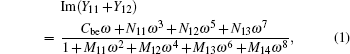
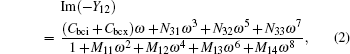
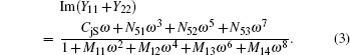
The junction capacitances are first extracted from the cold S-parameters measurement.[11] For the BE junction capacitance Cbe and BC junction capacitance Cbc, base voltage VB is swept from −1 V to 0.4 V under a fixed VC = 0 V. Similarly, for the CS junction capacitance CjS, VC is swept from −0.4 V to 1.5 V with a constant VB = VS = 0 V. Then the junction capacitance can be directly determined from the following non-linear rational function fitting over the whole frequency range:[11]
The coefficients Ni j and Mi j of other high-order terms each are a function of the circuit elements in Fig.
 | Fig. 2. Comparison between the measured (symbols) and fitting results (solid lines) of formulas (1)–(3) for 1 × 0.2 × 16 μm2 SiGe HBT biased at VB = VC = 0 V at room temperature. |
The substrate resistance RSU can be extracted by using the reported cold S-parameter approach.[12] The external collector resistance RCX can be determined through the convenient flyback method.[13] As for the emitter resistance RE, a novel extraction method has been proposed based on forward-Gummel measurements in our pervious study.[14] In the medium current region we can obtain

 | Fig. 3. Typical fitting result of Eq. ( |
As in our pervious study, the remaining model parameter RB can be obtained based on the nonlinear rational function fitting.[15] Taking a 4 × 1.2 × 20 μm2 SiGe HBT under off-states for example, as shown in Fig.
 | Fig. 4. Plots of RB and RCX versus Cbcx for 4 × 1.2 × 20 μm2 SiGe HBT in cut-off state. |
Through the given method as discussed above, the series resistances RCX, RSU, RE, and RB at each temperature can be extracted and the plots will be given below. By far, the problem of extracting each electrical element in the small-signal equivalent-circuit as shown in Fig.
In the HICUM model, the temperature dependence of model parameters is described via the physical quantities such as intrinsic carrier density, diffusivity or mobility. The temperature dependence of internal base resistance RB here depends on the carrier mobility in the neutral region. Then zero-bias resistance is described as:[16]

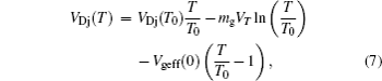
As in Ref. [11], all junction depletion capacitances are modeled in terms of the capacitance at zero bias Cj0, a built-in voltage VD and a grading coefficient zj. In HICUM the grading coefficient zj is assumed to be a constant and temperature-independent. To access the temperature dependence of built-in voltage VD, an auxiliary voltage VDj(T0) at given reference temperature T0 is calculated as indicated in Ref. [16] and given as follows:


The grading coefficient z here does not depend on temperature. As reported in Ref. [11], the well-known junction depletion capacitances can be modeled, respectively, as


It is noted that the built-in voltage VD is temperature dependent and the grading coefficient Zd is temperature-independent in the HICUM model, therefore, VD cannot be set as a constant similar to the case at room temperature. A novel parameter extraction flow for the depletion capacitances is recommend. First, the C–V characteristics at given reference temperature T0 is fitted directly, then the built-in voltage VD, zero-biased capacitance Cj0 and grading coefficient Zd will be obtained simultaneously if high accuracy exists. Otherwise, set VD as the default value, and extract the Cj0 and Zd from the C–V curve fitting. Finally, the values of VD and Cj0 at different temperatures can be determined from the corresponding C–V curve fitting under the assumption of Zd(T) = Zd(T0). Thus, the temperature dependences of VD(T) and Cj0(T) are obtained.
In HICUM the temperature dependence of model parameters is assumed to be irrelevant to device size, therefore, the extraction of temperature dependence for a single transistor geometry can also be applied to other-sized devices. The results for a 1 × 0.2 × 16 μm2 SiGe HBT are presented in this work. According to Eqs. (
 | Fig. 5. Temperature dependences of zero-bias capacitance and built-in voltage for BE junction. |
 | Fig. 6. Temperature dependences of zero-bias capacitance and built-in voltage for BC junction. |
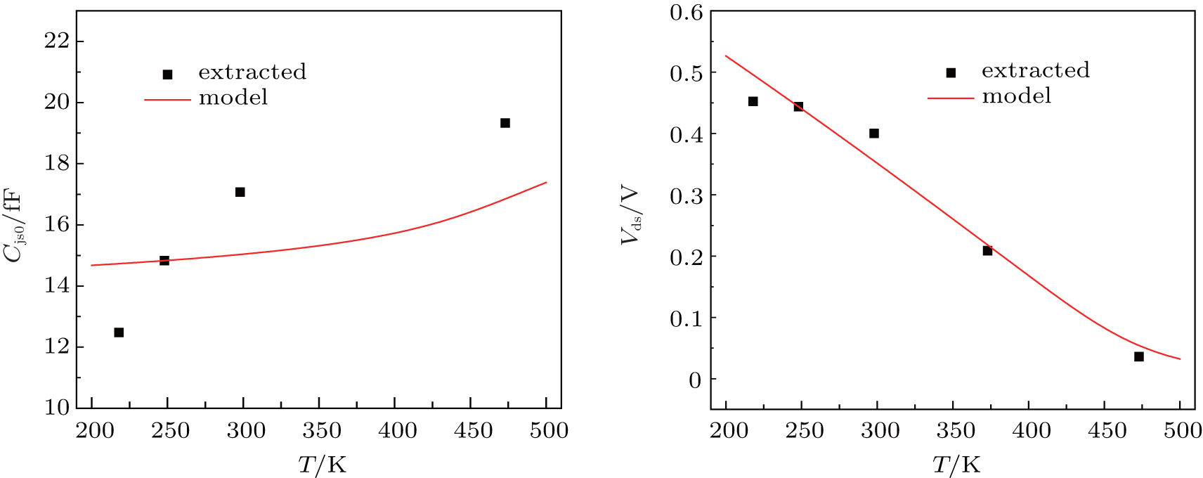 | Fig. 7. Temperature dependences of zero-bias capacitance and built-in voltage for CS junction. |
| Table 1. Extracted temperature coefficients for 1 × 0.2 × 16 μm2 SiGe HBT. . |
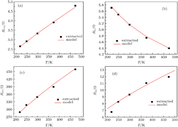
The temperature dependences of series resistances (RB, RCX, RE, and RSU) are shown in Fig.
 | Fig. 8. Temperature dependences of series resistances of (a) RCX, (b) RE, (c) RSU, and (d) RB. |
Because of the low doping concentration, the carrier mobilities in base, collector and substrate region are mainly dominated by the lattice vibration scattering, which shows a temperature dependence of T3/2 and increases with temperature increasing. Therefore, the carrier mobility in these regions decreases and the corresponding series resistances increase as temperature increases. While in the emitter region, it is the ionized impurity scattering that dominates the carrier mobility due to the higher doping concentration (generally at a level of 1020 cm−3). The ionized impurity scattering shows a temperature dependence of T3/2 and hence decreases with temperature increasing; as a result, the carrier mobility in the emitter region increases and then the emitter resistance RE decreases.
In this paper, the temperature dependences of small-signal model parameters for SiGe HBT HICUM under cut-off mode are presented from 218 K to 473 K. The depletion capacitances are extracted from the cold S-parameter measurements. Emitter resistance RE is obtained from the forward-Gummel measurement. Base resistance RB is gained from cold S-parameters based on the rational function fitting. Then the temperature dependences of model parameters are determined based on the established temperature formulas. The proposed method is verified with a 1 × 0.2 × 16 μm2 SiGe HBT and good agreement is obtained over the whole temperature range. These results provide a theoretical guide for designing devices and circuits of SiGe HBTs in a wide temperature range.
| 1 | |
| 2 | |
| 3 | |
| 4 | |
| 5 | |
| 6 | |
| 7 | |
| 8 | |
| 9 | |
| 10 | |
| 11 | |
| 12 | |
| 13 | |
| 14 | |
| 15 | |
| 16 |