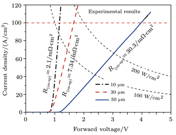
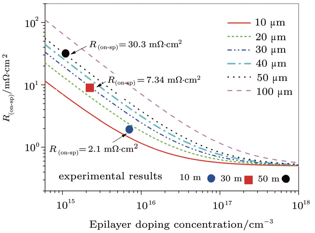
3.1. Forward characteristicsFigure 3 shows the forward current density–voltage (JF–V) characteristics of SiC SBDs fabricated with wafers No. 1–No. 3. The Schottky contact metals are Ti for the 1.2-kV and 3.3-kV class diode and Ni for the 5.0-kV class diode, respectively. Therefore, the turn-on voltages are 0.9 V for the 1.2-kV and 3.3-kV diodes and 1.2 V for the 5.0-kV class diodes, respectively. The Schottky barrier heights (SBHs) are estimated to be 1.2 eV and 1.6 eV for Ti/4H–SiC and Ni/4H–SiC, respectively, as derived from the low-current log–linear portion of the I–V curves (not shown). The values of forward voltage (VF) of the 1.2-kV, 3.3-kV, and 5.0-kV class SBDs are 1.15 V, 1.66 V, and 3.97 V respectively, when the forward current density (JF) is 100 A/cm2 at room temperature. The differential values of on-resistance (Ron−sp) at a current density of 100 A/cm2 are measured to be 30.3 mΩ·cm2, 7.34 mΩ·cm2, and 2.1 mΩ·cm2 for the 5.0-kV, 3.3-kV, and 1.2-kV classes respectively. As epitaxial thickness increases, the differential on-resistance significantly increases.
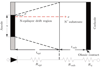
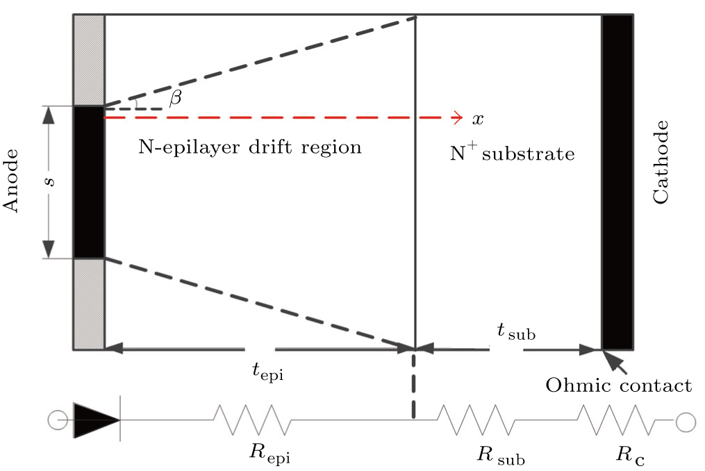
Owing to the current flow with the lateral effect in the epitaxial layer of power SBD device, the active area is larger than the anode area. Therefore, the forward conduction of 4H–SiC SBD can be a model as shown in Fig. 4 according to the current flow pattern in the SBD, where a parameter β is introduced to reflect the current lateral spreading effect. β values are 45° for 10-μm epilayer, 35° for 30-μm epilayer, and 30° for 50-μm epilayer, respectively, determined from the numerical simulations. Based on this model, the on-resistance can be divided into three different components: Ohmic contact resistance, epilayer spreading resistance, and substrate resistance. Thus the series resistance can be expressed as[23]

where
Repi is the epitaxial layer resistance,
Rc is the Ohmic contact resistance, and
Rsub is the substrate resistance. For the ideal
Ron−sp, the Ohmic contact resistance
Rc is usually neglected due to the fact that its value is far smaller than those of epitaxial layer resistance and substrate resistance. Therefore, the ideal
Ron−sp is shown as follows:

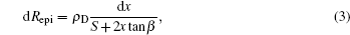
The epitaxial layer resistance is a trapezoid, which can be obtained by integration of d
Repi along the
x direction (as shown in Fig.
4) between the surface (
x = 0) and the N
+ substrate (=
tepi):
[23]
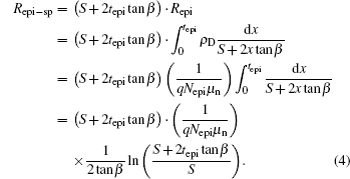
The substrate resistance can be calculated from
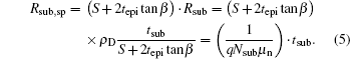
Therefore, the ideal
Ron−sp can be expressed as follows:
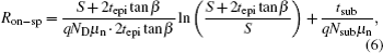
where
ND and
Nsub are the doping concentrations of the epilayer and substrate, respectively,
tepi is the thickness of the epilayer,
tsub is the thickness of substrate,
ρD is the resistivity of the 4H–SiC,
μn is the electron mobility of 4H–SiC, and
S = 2 mm is the Schottky junction width. Using this model, differential on-resistance can be calculated. The relationships between differential on-resistance and epilayer doping are plotted in Fig.
5 and compared with those obtained from experiments. It can be seen that the two sets of data show high consistency. Experimental results are very close to the ideal theoretical values of differential on-resistance determined by the epitaxial thickness and doping concentration.
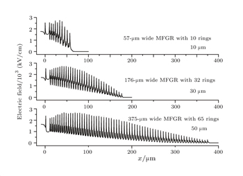
3.2. Reverse Blocking characteristicsThe reverse blocking characteristics of fabricated 4H–SiC SBDs based on epitaxial layers with different thickness values are in Fig. 6.
The dc blocking characteristic test is done in a probe station that is capable of testing the case of up to 10 kV. It can be seen that a sharp avalanche behavior is observed at reverse voltages of 1.4 kV (epitaxial thickness: 10 μm), 3.32 kV (epitaxial thickness: 30 μm), and 5.2 kV (epitaxial thickness: 50 μm), respectively. Figure 6 also shows the reverse leakage current density characteristics (JR–V) of diodes of the three types. The leakage current densities are 0.4 mA/cm2 at 1.2 kV, 0.96 mA/cm2 at 30 kV, and 0.96 mA/cm2 at 5.0 kV, respectively. Below the avalanche breakdown point, the JR rapidly increases with the reverse voltage increasing. The JR–V curves of those devices are produced by the typical thermionic field emission mechanisms, which leads to a barrier lowering effect proportional to the square of the electric field at the Schottky metal/semiconductor interface. The cases for dissipation powers per unit at 1 W/cm2, 5 W/cm2, and 15 W/cm2 for the fabricated three types of 4H–SiC SBDs are also presented in Fig. 6. In the case of the 5-kV 4H–SiC Schottky diode, the reverse power dissipation at room temperature is slightly less than 15 W/cm2, and for 1.2-kV and 3.3 kV-classes diodes, the reverse dissipation powers are 0.6 W/cm2 and 7.5 W/cm2 at reverse voltages of 1.2 kV and 3.0 kV, respectively.
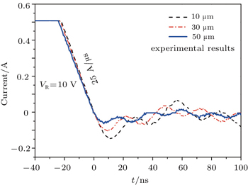
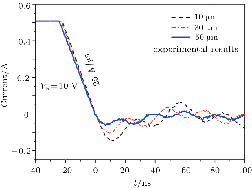
3.3. Reverse recovery characteristicsThe reverse recovery transients of the 1.2-kV, 3.0-kV, and 5.0-kV 4H–SiC SBDs at room temperature are shown in Fig. 7. Under the test conditions adopted, the devices are switched from the forward current of 0.5 A to the blocking state with a reverse bias of 10 V at a current rate-of-fall of 25 A/μs. For 5.0-kV 4H–SiC SBD, the diode has a reverse recovery time trr of 17.35 ns, a peak reverse current IRM(rec) of 0.064 A, and a reverse recovery charge Qrr of 1.402 nC. Table 2 summarizes the reverse recovery characteristics for the three types of SBDs. Since the reverse recovery current of a majority carrier diode (pure Schottky structure) is purely capacitive in nature, trr, IRM(rec), and Qrr are only dependent on the epitaxial doping concentration. As the epitaxial doping concentration increases, the reverse recovery transient time increases.
Table 2.
Table 2.
 Table 2. Reverse recovery characteristics of the fabricated 4H–SiC SBDs at room temperature. .
| Type/kV |
trr/ns |
IRM(rac))/A |
Qrr/nC |
Qc/nC |
| 1.2 |
27.59 |
0.168 |
3.460 |
3.612 |
| 3.3 |
22.47 |
0.108 |
2.452 |
2.522 |
| 5 |
17.35 |
0.064 |
1.402 |
1.516 |
| Table 2. Reverse recovery characteristics of the fabricated 4H–SiC SBDs at room temperature. . |
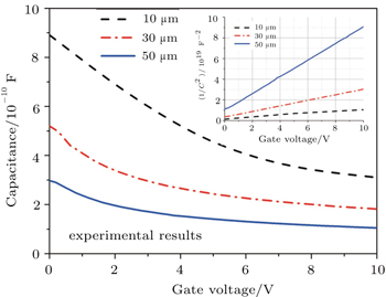
Figure 8 shows the high frequency (1 MHz) capacitance–voltage (C–V) curves for 10-, 30-, and 50-μm 4H–SiC SBDs. The inset displays the inverse square of capacitance (1/C2) as a function of gate voltage (V). The C–V data are measured over a gate voltage range from 0 V to −10 V. The epitaxial drift layer doping concentration ND can be extracted by employing a linear extrapolation of 1/C2 versus V. The extracted ND values for the No. 1, No. 2, and No. 3 wafers are presented in Table 1. Form the C–V curves, the total junction capacitance charge Qc can be extracted. For the three types of 4H–SiC SBDs measured, the average capacitive charge extrapolated to −10V is very close to the Qrr calculated from the reverse recovery transient, confirming that the reverse recovery current is entirely capacitive in nature.
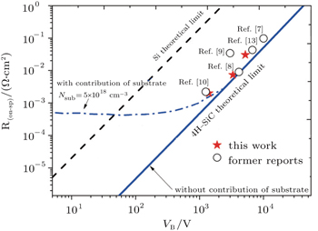
3.4. Tradeoff between specific on-resistance and breakdown voltageFor the unipolar power device such as Schottky diode, there is a tradeoff between specific on-resistance and breakdown voltage. For a certain rated breakdown voltage (BV), the ideal on-resistance of the device depends on the dielectric constant, the carrier mobility, and the critical electric field of semiconductor material. The on-resistance can be expressed as follows:

where
ɛs is the dielectric constant,
μn is the electron mobility,
EC is the breakdown electric field,
VB is the breakdown voltage,

is called the Baliga figure of merit (BFOM), which is commonly used to qualitatively evaluate the device characteristics. Figure
9 shows the curves of tradeoff between the specific on-resistance and the breakdown voltage. Solid diagonal lines in the figure represent the theoretical limits for silicon and 4H–SiC with the contribution of the substrate. The performances of a number of reported SiC power SBDs are also presented. The device fabricated in our group is also included for comparison. It can be seen that the performances of our present 4H–SiC SBDs are very close to the 4H–SiC theoretical limit. Moreover, the

values of our reported 4H–SiC SBDs are calculated to be 933 MW/cm
2, 1501 MW/cm
2, and 892 MW/cm
2, respectively. The best

value is obtained in the 3.32 kV device.


 , Tang Xiao-Yan2, ‡,