† Corresponding author. E-mail:
Project supported by the Key Technology Study for 16/14 nm Program of the Ministry of Science and Technology of China (Grant No. 2013ZX02303).
TiAlC metal gate for the metal-oxide-semiconductor field-effect-transistor (MOSFET) is grown by the atomic layer deposition method using TiCl4 and Al(CH3)3(TMA) as precursors. It is found that the major product of the TiCl4 and TMA reaction is TiAlC, and the components of C and Al are found to increase with higher growth temperature. The reaction mechanism is investigated by using x-ray photoemission spectroscopy (XPS), Fourier transform infrared spectroscopy (FTIR), and scanning electron microscope (SEM). The reaction mechanism is as follows. Ti is generated through the reduction of TiCl4 by TMA. The reductive behavior of TMA involves the formation of ethane. The Ti from the reduction of TiCl4 by TMA reacts with ethane easily forming heterogenetic TiCH2, TiCH=CH2 and TiC fragments. In addition, TMA thermally decomposes, driving Al into the TiC film and leading to TiAlC formation. With the growth temperature increasing, TMA decomposes more severely, resulting in more C and Al in the TiAlC film. Thus, the film composition can be controlled by the growth temperature to a certain extent.
The integrated circuit (IC) technology is the key in the modern information industry. In order to obtain high performance and low power, the feature size of the IC technology continually shrinks. For the 45 nm technology node, high dielectric material (high-k) and metal gate are introduced into the conventional metal–oxide–semiconductor (MOS) field-effect-transistor (FET).[1] For the 22 nm technology node, FinFET or Tri-gate structure is employed to continue equivalently scaling the MOSFET.[2,3] One of the main challenges for the introduction of high-k and metal gate is the appropriate work function of metal gate.[4–6] Titanium–aluminum-(Ti/Al) based metal has received much attention as N-type work function metal in the past few years. For example, TiAlN metal is highly considered as N-type metal gates in 45 nm and 32 nm product by Intel, due to its proper work function.[1,7] The Ti/Al-based metal has been widely deposited by physical vapor deposition (PVD) technique.[8,9] Although PVD has various advantages, its inherent nature does not allow conformal film growth, which is required for three-dimensional FinFET devices of 22 nm technology node and beyond. Atomic layer deposition (ALD) is a method based on sequential self-saturated surface reactions, leading to the controlled layer-by-layer growth of thin films at molecular level. The unique, generally self-limiting, growth mechanism of the ALD process gives better thickness control, thickness uniformity and conformality, than other deposition techniques.[10,11] Therefore ALD technology can offer the best solution to the problems accompanied by the scaling of MOSFET shrinking devices. However, ALD Ti/Al-based N-type work function metal is rather difficult to grow due to the precursor limit. There are only few publications about the N-type metal gate prepared by ALD until now. Ragnarsson et al. used a new ALD TiAl process to demonstrate conformal low threshold voltage bulk FinFET devices.[12] Jeon et al. and Kim et al. got ALD TiC–TiN film and ALD TiC film with acceptable effective work function (EWF).[13,14] In particular, the reaction mechanism of ALD N metal process is rarely reported.
In our previous work, we have grown the TiAlC film as N-type work function metal by thermal ALD.[15] The grown TiAlC film has an effective work function of 4.49 eV which is suitable for FinFET application. In this study, we investigated the reaction mechanism of the ALD TiAlC film grown by TiCl4 and Al(CH3)3 (TMA) reaction, based on the x-ray photoemission spectroscopy (XPS), Fourier transform infrared spectroscopy (FTIR), and scanning electron microscope (SEM) measurements.
TiAlC was grown using TiCl4 as Ti precursor and TMA as Al precursor by thermal ALD on Beneq ALD tool TFS200. Both of the TiCl4 and TMA were vaporized from liquid source containers kept at 21 °C and introduced into ALD reactor chamber by N2 carrier gas. The reaction pressure was about 1.5 millibar. One deposition cycle consists of TiCl4 pulse, N2 purge, TMA pulse, and N2 purge. The deposition temperature was changed in the range of 200 °C to 400 °C in the cold wall reactor. The gas flow was cross flow. The composition and bonding properties were measured by XPS and FTIR. The surface topography was evaluated by SEM.
Figure The composition of the as-deposited films grown at (a) 200 °C, (b) 300 °C, and (c) 400 °C measured by XPS. The composition of the as-deposited films grown at different temperatures measured by XPS.
Ti
C
Al
O
200 °C
61
2
1
36
300 °C
36
40
4
20
400 °C
34
51
8
7
Figure
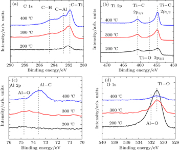
 | Fig. 2. XPS spectra of (a) C 1s, (b) O 1s, (c) Ti 2p, and (d) Al 2p of the as-deposited films grown at different temperatures. |
The oxygen component in the grown film is from the exposed atmosphere after film growth but not from the ALD process. This is because there is no oxygen supply in the ALD precursors (TiCl4 and TMA here) or in the ALD reaction chamber, so no oxygen should appear in the grown film. However, when the grown film is exposed to the atmosphere, the film can be oxidized by the O2 in the atmosphere. As a result, the oxygen component should be excluded from each grown film. In other words, the film grown at 200 °C is Ti with nearly negligible C. The film grown at 300 °C and 400 °C is TiAlC. The oxidation of TiAlC film can be avoided in the real fabrication of MOS devices. In the device fabrication process, after the growth of TiAlC film, ALD TiN is in situ deposited in the same ALD chamber. Then the TiN/TiAlC sample is transferred from ALD chamber to another ALD chamber (for ALD W) within 2 min for metal W deposition. The metal W can protect the TiN/TiAlC films from being oxidized, so the oxidation of ALD TiAlC is rather negligible.
Figure
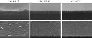
 | Fig. 3. The cross section (top) and surface morphology (bottom) of the as-deposited film grown at (a) 200 °C, (b) 300 °C, and (c) 400 °C. |
 | Fig. 4. The surface roughness pictures of the as-deposited films grown at (a) 200 °C, (b) 300 °C, and (c) 400 °C. |
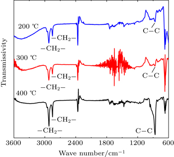
In order to further investigate the growth mechanism, the FTIR spectra were measured. Figure
According to the results described above, we make the following reasonable speculation about the growth mechanism. The reductive behavior of Al(CH3)3 involves the formation of ethane, which has been found by other researchers on ALD manufacturing Cu film.[16] The XPS results suggest that the pure titanium metal was generated through the reduction of TiCl4 by TMA. Then Ti reacts with ethane forming heterogenetic TiCH2, TiCH=CH2, and TiC fragments.[17] Meanwhile, TMA thermally decomposes, driving Al doping into the film and leading to TiAlC formation. The higher the temperature is, the easier the reaction happens. The above conclusion is further confirmed by FTIR, where the signals of −CH=CH2 (around 860 cm−1) and −CH2 (approximately 2918 cm−1, 2850 cm−1) exist in all samples, and the signals are enhanced obviously as the temperature increases.
TiAlC metal gate was grown by using TiCl4 and TMA as precursors. Ti is generated through the reduction of TiCl4 by TMA. The reductive behavior of TMA involves the formation of ethane. The Ti from the reduction of TiCl4 by TMA reacts with ethane forming heterogenetic TiCH2, TiCH=CH2, and TiC fragments. In addition, TMA thermally decomposes, driving Al into the TiC film and leading to TiAlC formation. With the growth temperature increasing, TMA decomposes more severely, leading to more C and Al in the TiAlC film. Thus, the film composition can be controlled by the growth temperature to a certain extent.
| 1 | |
| 2 | |
| 3 | |
| 4 | |
| 5 | |
| 6 | |
| 7 | |
| 8 | |
| 9 | |
| 10 | |
| 11 | |
| 12 | |
| 13 | |
| 14 | |
| 15 | |
| 16 | |
| 17 |


