Influence of trap-assisted tunneling on trap-assisted tunneling current in double gate tunnel field-effect transistor
[Jiang Zhi†,  , Zhuang Yi-Qi, Li Cong, Wang Ping, Liu Yu-Qi]
, Zhuang Yi-Qi, Li Cong, Wang Ping, Liu Yu-Qi]
|
|


† Corresponding author. E-mail:
Project supported by the National Natural Science Foundation of China (Grant Nos. 61574109 and 61204092).
Trap-assisted tunneling (TAT) has attracted more and more attention, because it seriously affects the sub-threshold characteristic of tunnel field-effect transistor (TFET). In this paper, we assess subthreshold performance of double gate TFET (DG-TFET) through a band-to-band tunneling (BTBT) model, including phonon-assisted scattering and acoustic surface phonons scattering. Interface state density profile (Dit) and the trap level are included in the simulation to analyze their effects on TAT current and the mechanism of gate leakage current.
Tunnel Field-Effect Transistors (TFETs) are a new concept of device that has been proposed as a promising option to conventional MOSFET. Owing to different operating principles, the TFETs have attracted much attention because of their steep subthreshold swing (SS < 60 mV/dec).[1–4] One significant task for TFETs is to study which factors deteriorate sub-threshold characteristics. However, in many papers just the effects of the trap density on subthreshold swing (SS) and off-state current (Ioff) were studied, and interface traps (ITs) and phonon scattering were considered for TFET by a few authors.[5–9] Furthermore, there are few reports of physically detailed effect of gate leakage current on TFET.
In general, the tunneling happens uniformly along the gate on the source side, and high-κ gate insulator as well as lattice mismatch in source-channel junction could induce those traps existing at the interface. Such an important issue is that the influences of trap level and phonon-assisted tunneling on the DG-TFET need further physical insight. In this paper, we focus on the TAT and gate leakage current behavior in DG-TFET. It is shown that different positions of trap and phonon scattering can result in the degradations of the SS and TAT current.
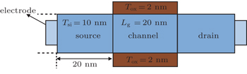
In this paper, the device structure under investigation is an all Si double-gate n-TFET (DG-nTFET), as illustrated in Fig.
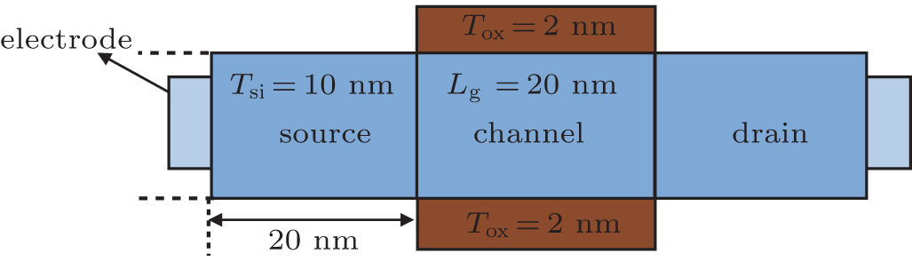 | Fig. 1. Device structure of a DG n-type TFET. |
To elucidate the relationship between TAT current and phonon scattering, and that between gate leakage current and tunneling in DG-nTFET, the device simulation setup includes the dynamical nonlocal-path band-to-band tunneling (BTBT) model, dynamic nonlocal path trap-assisted tunneling, enhanced Lombardi model with high-κ degradation, a fully quantum-mechanical gate leakage current tunneling model, and hot-carrier injection model. When oxide is thinner than 3 nm, the gate leakage and mobility degradation must be considered. In the TAT simulations, a constant tunneling mass (me = 0.19m0, mh = 0.2m0) is used, and nonlocal BTBT model (A = 4×1014 cm−3·s−1, B = 2×10⁷ V·cm−1) is also adopted. Carrier bulk lifetime and trap capture cross section are 0.1 μs and 10−10 cm2 respectively. In addition, carrier injection model calculates the hot-carrier injection current by using the nonequilibrium energy distribution which contributes to distinguishing the influences of two different mechanisms on gate leakage current. Even more importantly, the influences of optical phonon (OP) assisted inelastic tunneling and acoustic phonon (AP) scattering on the carrier mobility could be effectively studied. In all DG-nTFET simulations in this paper we assume VDS = 0.5 V.
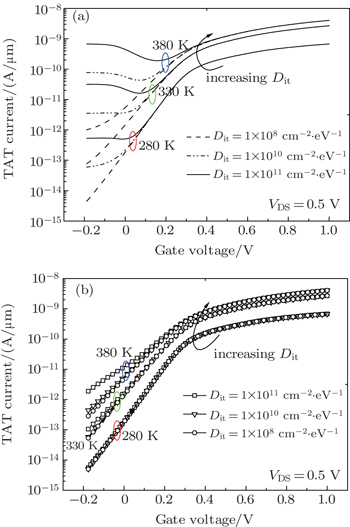
The simulated TAT currents in this work are plotted in Fig.
 | Fig. 2. TAT characteristics of the DG-nTFET, showing variable interface trap density Dit with uniquely different temperature dependences in a range of 280 K–380 K. (a) Influence of trap location (gate/channel) on the TAT characteristic. (b) Influence of trap location (source/channel) on the TAT characteristic. |
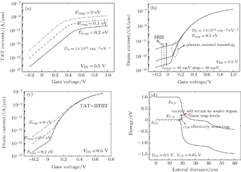
To obtain further insight, we study the influence of trap levels on TAT characteristics of DG-nTFET with Dit = 1010 cm−2·eV−1. When trap level turns closer to valence band at the gate/channel interface in source region, the simulation results display that TAT current would increase as shown in Fig.
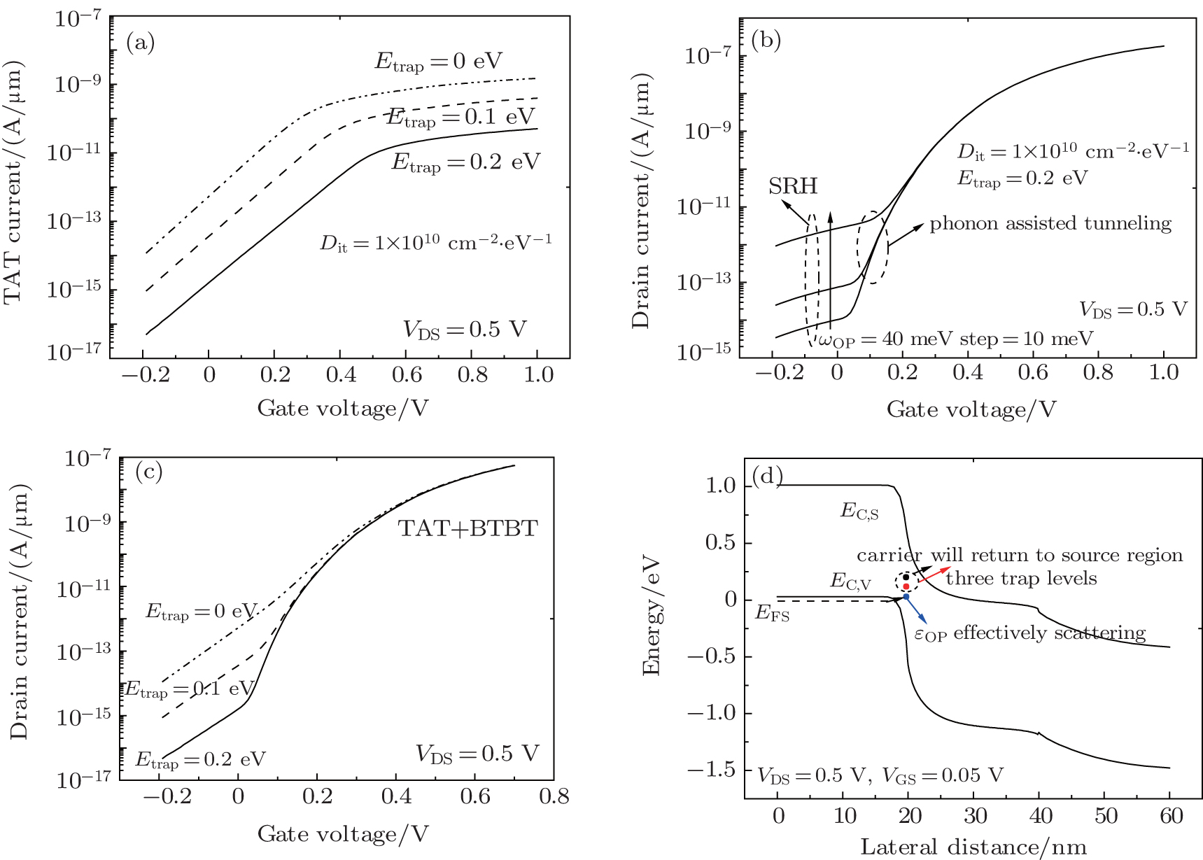 | Fig. 3. Influences of the trap energy level on the TAT current through gate/channel interface trap. (a) The TAT current increases with increasing proximity of the trap level to the source valence band. (b) Off-state and TAT current increase with increasing the scattering phonon energy. (c) The TAT current is lowest when trap level is far away from the valence band with BTBT and TAT. (d) Energy-position of one-dimensional DG-nTFET with phonon-assisted scattering. It can be clearly seen that phonon absorption assisted transport occurs at the gate/channel interface. |
Here, a close match with experimental data is obtained when considering BTBT component and TAT component[12] as shown in Fig.

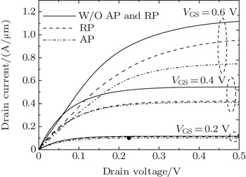
When the gate voltage is over threshold voltage, the remote phonons (RPs) scattering and acoustic phonons (APs) scattering begin to have an influence, which stem from the high-κ dielectrics. Carriers are scattered into trap level, followed by thermal emission into the conduction band. An increase in VDS results in reducing the electron concentration in the channel, and the electrons are now pulled back to the end of the drain. The mobility would suffer RP scattering. Figure
 | Fig. 4. IDS–VDS characteristics for the DG-nTFET at VGS = 0.2 V, 0.4 V, and 0.6 V in the cases with and without scattering. Source/channel interface scattering (AP) and electron mobility scattering (RP) are considered independently. These elastic scatterings would reduce BTBT rate and the mobility. |
In many cases, there are few researchers to discuss the gate leakage current. On-state current can be effectively and easily improved by using a thinner high-κ gate dielectric. However, this method has a major disadvantage, that is, the gate leakage current. The leakage floor would reduce device reliability. For DG-nTFET, the leakage floor can be divided into hot-carrier injection current and direct tunneling current. Direct tunneling and hot-carrier injection are the main gate leakage mechanism for oxides thinner than 3 nm. With the decrease of the device size, hot carrier effect failure has received much attention nowadays, it becomes one of the main failure mechanisms, especially in TFET.
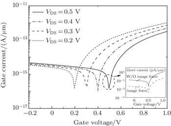
A comparison of the apparent shift in the onset of gate leakage among different VDS values is shown in Fig.
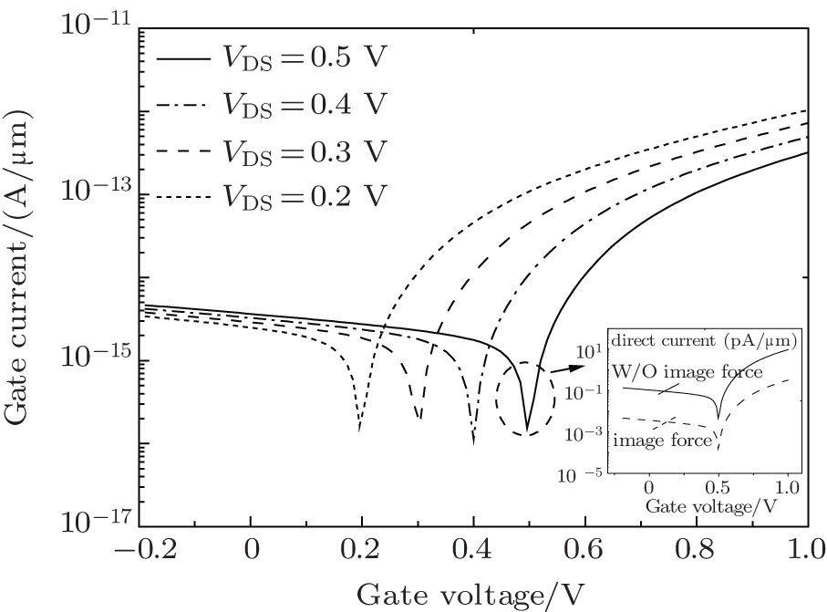 | Fig. 5. Gate leakage characteristics for different values of the drain voltage. The inset shows the image force can reduce the leakage floor by two orders of magnitude. |
When the gate oxide thickness reduces to 2 nm, oxide barriers are easily affected by the image force. The image force can reduce the tunneling barrier, hence, the gate direct tunneling current decreases as shown in the inset of Fig.
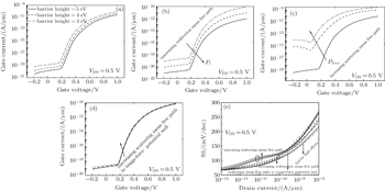
Figure

 | Fig. 6. Gate leakage characteristics of the DG-nTFET, showing (a) barrier height dependence: higher barrier can effectively reduce the hot-carrier injection current; (b) redirection mean free path dependence: leakage floor can be limited by longer redirection distance; (c) scattering mean free path in semiconductor: the scattering rate of hot-carrier would be increased by increasing the scattering path; (d) scattering length dependence in the image-force potential well: this effect is similar to electron traveling a distance in semiconductor, but it is not obvious; (e) SS versus drain current for different free paths, barrier heights and image-forces. |
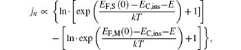
In addition, the gate leakage current is also influenced by scattering mean free path λ in semiconductor. The probability is given by the following expression:[13]


In this paper, we present the TAT current and gate leakage current characteristics of all-Si DG-nTFET. Based on different defect levels, phonon energies and trap densities, transfer characteristics of subthreshold which suffers the influence of phonon scattering are studied. The phonon with higher scattering energy and the phonon closer to the valence band would deteriorate SS and off-state current. The DG-nTFET leakage floor is vulnerable to not only barrier height of semiconductor/oxide, but also scattering mean free path. Leakage floor can be improved by increasing the barrier height and a robust surface processing.
| 1 | |
| 2 | |
| 3 | |
| 4 | |
| 5 | |
| 6 | |
| 7 | |
| 8 | |
| 9 | |
| 10 | |
| 11 | |
| 12 | |
| 13 | |
| 14 |