A uniform doping ultra-thin SOI LDMOS with accumulation-mode extended gate and back-side etching technology
Zhang Yan-Hui1, Wei Jie1, Yin Chao1, Tan Qiao1, Liu Jian-Ping1, Li Peng-Cheng1, Luo Xiao-Rong1, 2, †,
State Key Laboratory of Electronic Thin Films and Integrated Devices. University of Electronic Science and Technology of China, Chengdu 610054, China
Science and Technology on Analog Integrated Circuit Laboratory, Chongqing 400060, China


† Corresponding author. E-mail: xrluo@uestc.edu.cn

Project supported by the National Natural Science Foundation of China (Grant Nos. 61176069 and 61376079).

Abstract
Abstract

A uniform doping ultra-thin silicon-on-insulator (SOI) lateral-double-diffused metal-oxide-semiconductor (LDMOS) with low specific on-resistance (Ron,sp) and high breakdown voltage (BV) is proposed and its mechanism is investigated. The proposed LDMOS features an accumulation-mode extended gate (AG) and back-side etching (BE). The extended gate consists of a P– region and two diodes in series. In the on-state with VGD > 0, an electron accumulation layer is formed along the drift region surface under the AG. It provides an ultra-low resistance current path along the whole drift region surface and thus the novel device obtains a low temperature distribution. The Ron,sp is nearly independent of the doping concentration of the drift region. In the off-state, the AG not only modulates the surface electric field distribution and improves the BV, but also brings in a charge compensation effect to further reduce the Ron,sp. Moreover, the BE avoids vertical premature breakdown to obtain high BV and allows a uniform doping in the drift region, which avoids the variable lateral doping (VLD) and the “hot-spot” caused by the VLD. Compared with the VLD SOI LDMOS, the proposed device simultaneously reduces the Ron,sp by 70.2% and increases the BV from 776 V to 818 V.

1. Introduction

For high voltage power metal–oxide–semiconductor field-effect transistors (MOSFETs), two major targets are to reduce the power dissipation and enhance the breakdown voltage (BV), thereby realizing the trade-off between the specific on-resistance (Ron,sp) and BV.[1,2] Many approaches including the reduced surface field (RESURF) and super junction (SJ) are used to realize the targets. However, the Ron,sp in SJ and RESURF devices is strongly dependent on the drift doping concentration (Nd).[36] In order to realize high BV for the thin SOI, the variable lateral doping (VLD) and back-side etching (BE) are typical technologies by achieving a uniform lateral electric field.[79] However, the VLD technique leads to a “hot-spot” on the source side where the resistance is large for the low doping concentration[10] and its fabrication process needs a long-time high-temperature annealing.[11] The BE technique removes the substrate-assisted depletion effect (SAD), which results in a sharp decrease in Nd and restricts the current capability. Therefore, the BE technique was mainly applied to the IGBT with a conduction modulation effect.[9,12]

In this paper, an ultra-thin SOI LDMOS with an accumulation gate (AG) over the drift region and back-side etching (BE) (AG-BE SOI LDMOS) is proposed. Except for complex external control circuits, a high density electron accumulation layer is formed along the drift surface in the on-state.[13] This not only reduces the Ron,sp significantly, but also makes Ron,sp nearly independent of the doping concentration of the drift region. The BE technique allows a uniform doping concentration in the drift region to obtain high BV. The combination of the accumulation layer and the uniform doping concentration profile not only reduces the Ron,sp and the process difficulty, but also solves the “hot-spot” problem in the ultra-thin device with the VLD technology. The MEDICI simulator is used to study the mechanism of the AG-BE SOI LDMOS. The results demonstrate that the proposed device possesses good performances.

2. Device structure and mechanism

Figure 1 shows the schematic of the cross section of the AG-BE SOI LDMOS. The novel SOI LDMOS is characterized by the AG over the drift region and BE of the substrate. Note that the AG structure consists of a P-region and two diodes (D1 and D2) in series, and its two ends connect with the gate electrode and the drain electrode respectively. The substrate under the drift region is etched. The x and y directions are marked. Ld is the length of the drift region; ttop, tsi, and tbox represent the thickness values of the AG layer, the drift region and the buried oxide, respectively; Nd is the doping concentration of the drift region, and Np is the doping concentration of the P– region in the AG structure.

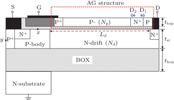
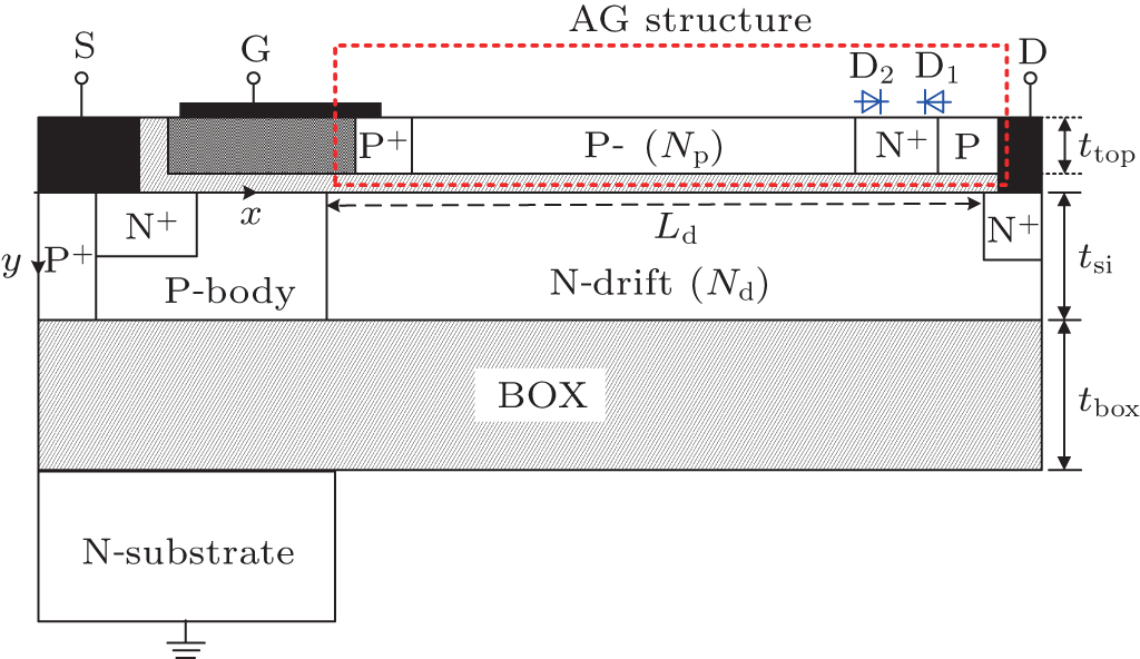
Fig. 1. Schematic diagram of cross section of the AG-BE SOI LDMOS.

Figure 2 illustrates the operation mechanism of the novel SOI lateral-double-diffused metal-oxide-semiconductor. An MIS-like structure is formed by the N-drift region, the gate dielectric layer and the P- region of the AG structure. In the on-state with VGD > 0, the diode D1 principally sustains the gate-drain voltage (VGD), and an electron accumulation layer is formed along the surface of the N-drift region. The accumulation layer forms an ultra-low resistance current path as shown in Fig. 2(a). Therefore, most of the current flows through the accumulation layer and thus the Ron,sp is almost independent of Nd. In the off-state, VDS = VDG > 0, the P- region of the AG and N-drift region works like an SJ with a thin oxide layer as depicted in Fig. 2(b). Then Nd increases and the Ron,sp further decreases due to the charge compensation.[14,15] Note that the diode D1 or D2 is reverse-biased to sustain the gate-drain voltage drop (VGD) in the on-state or off-state respectively, which ensures a lower leakage current in the top layer than that in Ref. [16].

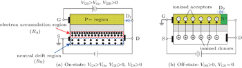
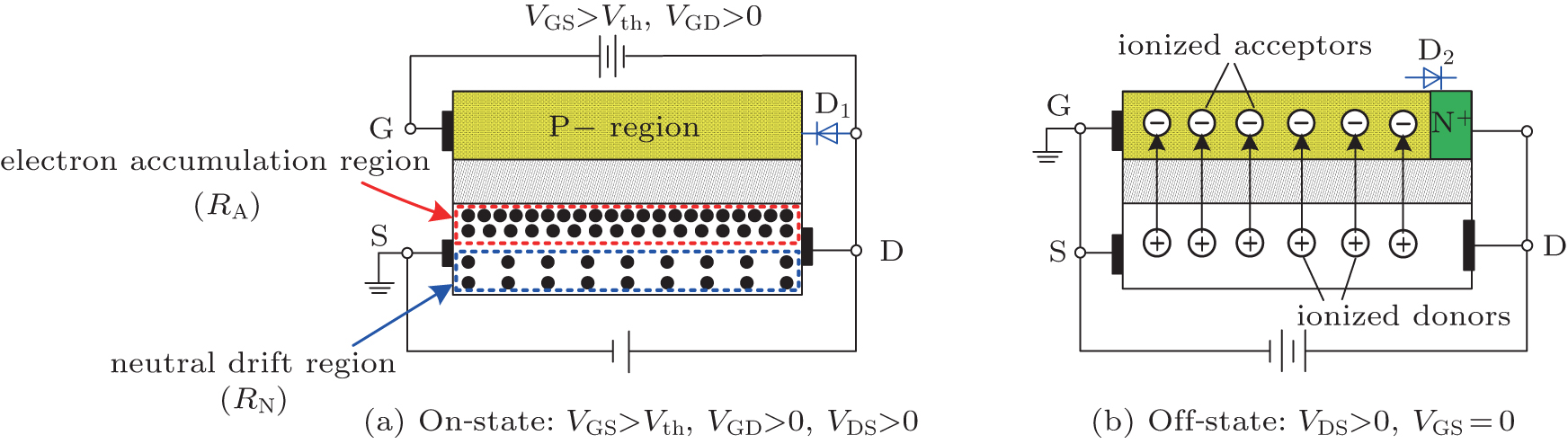
Fig. 2. Operation mechanism. (a) On-state: VGS > Vth, VGD > 0, VDS > 0; (b) off-state: VDS > 0, VGS = 0, and reverse biased D2 sustains the VDG.

In our simulations, the physical models of CONSRH, AUGER, BGN, FLDMOB, SRFMOB, IMPACT.I, and CCSMOB are mainly used, and the NEWTON solution method is used with two types of carriers. The dimensional parameters of the novel structure are set as follows: Ld = 46 μm, ttop = tsi = 0.2 μm, and tbox = 1 μm.

Figure 3 shows the equipotential contours and the lateral component of surface electric field (Ex) for the AG-BE silicon-on-insulator lateral-double-diffused metal-oxide-semiconductor, ultra-thin silicon-on-insulator lateral-double-diffused metal-oxide-semiconductor with accumulation extended gate and VLD profile in drift region (AEG-VLD SOI LDMOS),[17] ultra-thin silicon-on-insulator lateral-double-diffused metal-oxide-semiconductor with VLD profile in drift region (VLD SOI LDMOS) and conventional ultra-thin silicon-on-insulator lateral-double-diffused metal-oxide-semiconductor with a uniform doped drift region. For ultra-thin SOI devices in Figs. 3(a)3(d), the structure with VLD or BE can generate near-ideal potential distributions in the drift region as shown in the red dashed boxes in Figs. 3(a)3(c) respectively. The BE technique releases the equipotential lines below the buried oxide as shown in the black rectangle in Fig. 3(a); however, the equipotential contours of the VLD and AEG-VLD structure terminate in the bottom interface of the buried oxide as indicated in Figs. 3(b)3(c). In other words, the BE removes the vertical voltage drop and avoids vertical premature breakdown, which indicates that the BV is almost independent of the thickness values of the drift region and the buried oxide. Figure 3(e) shows that Ex for the conventional device is zero in the middle, fortunately, the AG-BE or the VLD not only enhances the Ex but also makes the field distribution more uniform. Furthermore, the BE technique almost removes the electric field peak on the drain side (Exd), and the AG enhances the Ex in the middle more effectively than the VLD. Therefore, the BV of the AG-BE silicon-on-insulator lateral-double-diffused metal-oxide-semiconductor increases from 776 V to 818 V for the VLD silicon-on-insulator lateral-double-diffused metal-oxide-semiconductor.

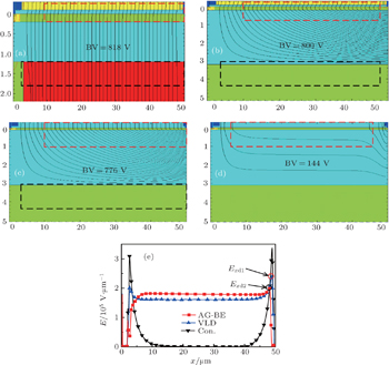
Fig. 3. Equipotential contour distributions (20 V/contour) at breakdown (optimally) for (a) AG-BE SOI LDMOS (BV = 818 V), (b) AEG-VLD SOI LDMOS (BV = 800 V), (c) VLD SOI LDMOS (BV = 776 V), and (d) conventional SOI LDMOS (BV = 144 V); (e) lateral surface electric field component.
3. Results and discussion

Figure 4 compares the on-state current densities of the AG-BE SOI LDMOS, the VLD SOI LDMOS and the JFP-BE SOI LDMOS at x = 5 μm. The JFP-BE SOI LDMOS features a junction field plate (JFP)[18] and BE. In the blocking state, the P-region in the JFP generates additional depletion in the N-drift region and increases the Nd, which is almost the same as the scenarios in AG-BE devices, so the same optimal Nd = Np = 4×1016 cm−3 and the same BV are obtained for the JFP-BE and AG-BE devices. For the AG-BE SOI LDMOS, the resistance in the drift region (RD) contains the accumulation layer resistance (RA) and the neutral drift region resistance (RN) in parallel, and RARN because of the high density accumulation electrons. Therefore, the surface current density of the accumulation layer is three orders higher than that in the neutral drift region, and the current through the accumulation layer (IA) is approximately 88% of the total current (ID) as shown in Fig. 4. Owing to the same Nd, the RN of the AG-BE device is the same as that of the JFP-BE device, and thus the current density IN values in the neutral drift region for AG-BE and JFP-BE devices are consistent. The IN value of the VLD SOI LDMOS is higher than those of AG-BE and JFP-BE SOI LDMOS, because the SAD effect of the VLD SOI LDMOS allows a higher Nd. Consequently, compared with the cases of the other two devices, the Ron,sp of the AG-BE device drops significantly and is almost independent of Nd. The Ron,sp values of the AG-BE SOI LDMOS, the VLD SOI LDMOS, and the JFP-BE SOI LDMOS are 38.1 mΩ·cm2, 106 mΩ·cm2, and 191 mΩ·cm2, respectively. However, the Ron,sp of SOI LDMOS only with the BE technique is over 5500 mΩ·cm2 at the same cell pitch.

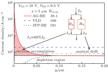
Fig. 4. Current density distributions of three devices at x = 5 μm.
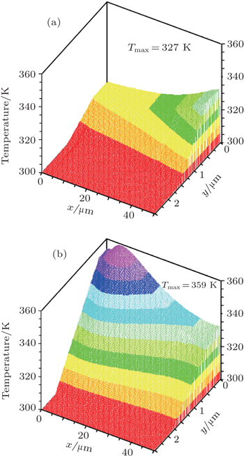
Figures 5(a) and 5(b) show the three-dimensional (3D) temperature distributions of the AG-BE SOI LDMOS and the VLD SOI LDMOS at the same power density (P) of P = 1 mW/ μm, respectively. Obviously, the VLD SOI LDMOS suffers a serious “hot-spot” on the source side for the low doping concentration herein. By contrast, the AG-BE SOI LDMOS obtains a lower and more uniform temperature in the drift region due to the lower and more evenly-distributed RD. Because of the accumulation layer and uniform drift doping, the maximum temperature of the AG-BE SOI LDMOS decreases from 359 K to 327 K of the VLD SOI LDMOS.

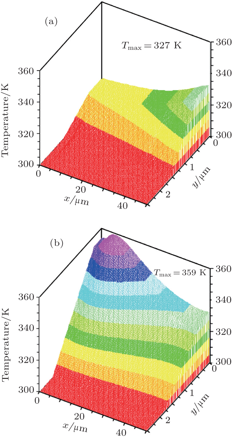
Fig. 5. 3D temperature distributions at P = 1 mW/ μm for (a) AG-BE SOI LDMOS and (b) VLD SOI LDMOS.
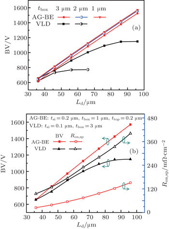
Figures 6(a) and 6(b), respectively, show the influences of the Ld and tbox on the BV and those of BV and Ron,sp on Ld for the AG-BE SOI LDMOS and VLD SOI LDMOS. As illustrated in Fig. 6(a), the BV of the VLD SOI LDMOS is saturated for Ld > 45 μm with tbox = 2 μm and Ld > 75 μm with tbox = 3 μm, because its vertical BV is limited by the thickness values of the drift region and the buried oxide layer. However, the BV of AG-BE SOI LDMOS is determined by the lateral BV and increases approximately linearly with increasing Ld, thereby avoiding the limit of the vertical BV as shown in Figs. 6(a) and 6(b). Therefore, the optimized tbox values for the novel device and the VLD SOI LDMOS are 1 μm and 3 μm, respectively. Moreover, owing to the accumulation layer, the Ron,sp of the novel device is lower and increases more slowly with the increasing Ld than that of VLD SOI LDMOS as shown in Fig. 6(b). Figure 7 compares the Ron,sp versus BV for this work with existing RESURF LDMOSFETs and SJ LDMOSFETs. The AG-BE SOI LDMOS obtains a superior trade-off between the BV and Ron,sp to the others.

Fig. 6. (a) Influences of Ld and tbox on BV, (b) dependences of the BV and Ron,sp on Ld.
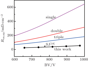
Fig. 7. Comparison of results between this work and the others.
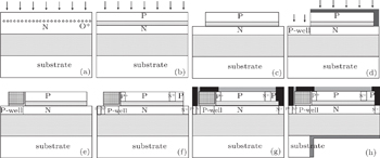
Figure 8 shows the feasible key fabrication steps of the AG-BE SOI LDMOS. The process to obtain the monocrystalline silicon in the AG is based on the SIMOX technology. Step (a) is for the process of the oxygen ion implantation,[20] followed by the annealing process to form the field oxide layer, leaving monocrystalline silicon on the oxide. Step (b) is for boron implantation to form the P-region in AG. Steps (c) and (d) are to form the active region and P-well by etching and boron implantation. Steps (e)–(g) are for the processes to form the poly-gate, contact regions and electrodes respectively. Finally, front-passivation is accomplished and followed by a substrate back-etching and subsequent back-passivation.[21,22]

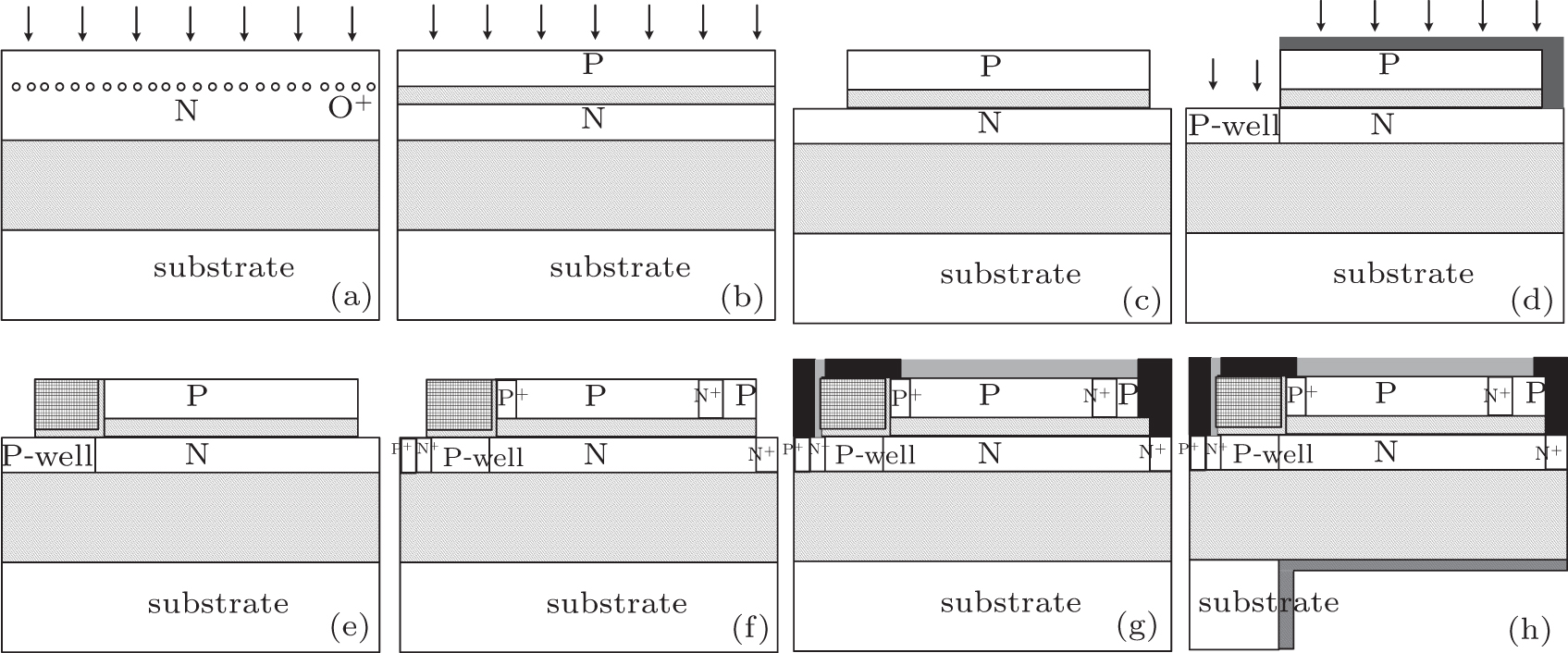
Fig. 8. Feasible key fabrication steps for forming the AG-BE SOI LDMOS: (a) oxygen ion implantation and annealing process to form the gate dielectric layer, (b) boron implantation to form the P-region in AG, (c) etching to form the active region, (d) boron implantation to form the P-well, (e) forming the gate oxide and poly-gate, (f) impurity implantation and annealing to form the contact regions, (g) forming the electrodes and front passivation, and (h) substrate back-etching and back passivation.
4. Conclusions

A novel SOI LDMOS with an accumulation gate and back-side etching is proposed and investigated by simulation. A high density electron accumulation layer generated by the AG provides a low resistant current path, which not only reduces the Ron,sp, but also flattens the surface temperature. On the other side, the back-side etching not only achieves a near-ideal potential distribution with a uniform doping concentration in the drift region but also avoids vertical premature breakdown. Compared with the VLD SOI LDMOS, the novel device combining the accumulation gate and back-side etching reduces the Ron,sp by 70.2% and improves the BV from 776 V to 818 V.

Reference
1Ludikhuize A W2001 Proceedings of the 31st European, IEEE Solid-State Device Research ConferenceSeptember 11–13, 2001p. 3510.1109/ESSDERC.2001.195201
2Iqbal M M Udrea F Napoli E2009IEEE Proceedings of the 21st International Symposium on Power Semiconductor Devices and ICsJune 14–18, 2009Barcelona, Spainp. 24710.1109/ISPSD.2009.5158048
3Ming QLi Y FZhou XLi Z JZhang B 2014 IEEE Electron Dev. Lett. 35 774
4Chen X BU S Patent 5216275 [1993-06-01]
5Chen YLiang Y CSamudra G SXin YBuddharaju K DFeng H H 2008 IEEE Trans. Electron Dev. 55 211
6Luo X Wei J Shi X Zhou K Tian R Zhang B Li Z 2014 IEEE Trans. Electron Dev. 61 4304
7Merchant S Arnold E Baumgart H Mukherjee S Pein H Pinker R1991 IEEE Proceedings of the 3rd International Symposium on Power Semiconductor Devices and ICsApril 22–24, 1991Maryland, USAp. 3110.1109/ISPSD.1991.146060
8Luo X RWei JShi X LZhou KTian R CZhang BLi Z J 2014 IEEE Trans. Electron. Dev. 61 4304
9Udrea F Trajkovic T Lee C Garner D Yuan X Joyce J Udugampola N Bonnet G Coulson D Jacques R Izmajlowicz M van der Duijn Schouten N Ansari Z Moyse P Amaratunga G A J 2005 IEEE Proceedings of the 17th International Symposium on Power Semiconductor Devices and ICsSanta Barbara, USAp. 26710.1109/ISPSD.2005.1488002
10Leung Y KAmit K PKenneth E GJames D PWong S S 1997 IEEE Electron Dev. Lett. 18 414
11Zhang S Sin J K O Lai T M L Ko P K 1999 IEEE Trans. Electron Dev. 46 1036
12Trajkovic T Udrea F Lee C Udugampola N Pathirana V Mihaila A Amaratunga G A J2008IEEE Proceedings of the 20th International Symposium on Power Semiconductor Devices and ICsMay 18–22, 2008Oralando, USAp. 32710.1109/ISPSD.2008.4538965
13Lyu X JChen X B 2013 IEEE Trans. Electron Dev. 60 3821
14Chen X BSin J K O 2001 IEEE Trans. Electron Dev. 48 344
15Gan K P Liang Yung C Samudra Ganesh S Xu S M Liu Y2001Power Electronics Specialists ConferenceJune 17–21, 2001Vancouver, Canadap. 215610.1109/PESC.2001.954439
16Vestling L Edholm B Olsson J Tiensuu S Soderbarg A1997Proceedings of the International Symposium on Power Semiconductor Devices & IC’sMay 26–29, 1997Weimar, Germanyp. 4510.1109/ISPSD.1997.601427
17Wei J Luo X Zhang Y Li P Zhou K Li Z Zhang B2015 Proceedings of the International Symposium on Power Semiconductor Devices and IC’sMay 10–14, 2015Hong Kong, Chinap. 18510.1109/ISPSD.2015.7123420
18Luo Y CLuo X RHu G YFan Y HLi P CWei JTan QZhang B 2014 Chin. Phys. B 23 077306
19Lin ZChen X B 2015 IEEE Electron Dev. Lett. 36 588
20Matsumura ASasaki TKitahara KUS patent 0170940 [2003].
21Udrea F Trajkovic T Amaratunga G A J2004Proceedings of IEEE Int. Electron DevicesDecember 13–15, 2004San Francisco, USAp. 45110.1109/IEDM.2004.1419185
22Udrea F Amaratunga GUS patent 6703684 [2004]