A uniform doping ultra-thin SOI LDMOS with accumulation-mode extended gate and back-side etching technology
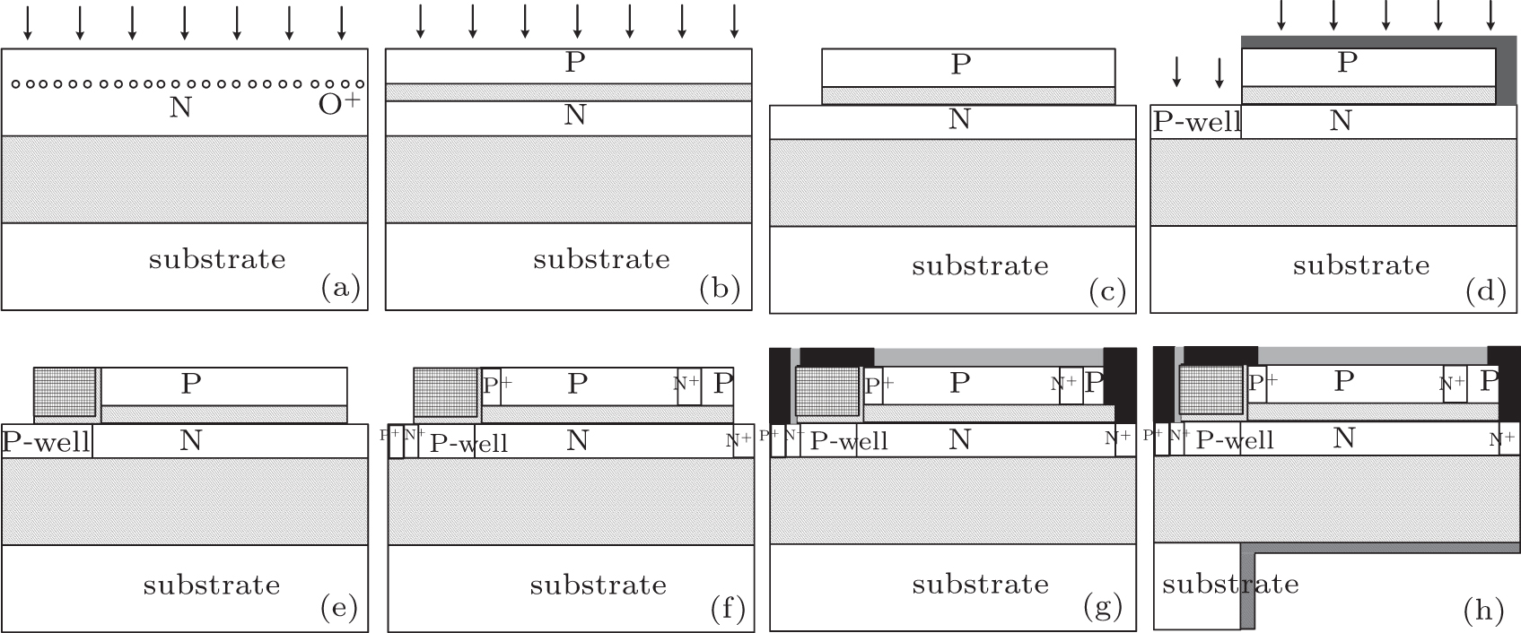
Feasible key fabrication steps for forming the AG-BE SOI LDMOS: (a) oxygen ion implantation and annealing process to form the gate dielectric layer, (b) boron implantation to form the P-region in AG, (c) etching to form the active region, (d) boron implantation to form the P-well, (e) forming the gate oxide and poly-gate, (f) impurity implantation and annealing to form the contact regions, (g) forming the electrodes and front passivation, and (h) substrate back-etching and back passivation.

