†Corresponding author. E-mail: hailu@nju.edu.cn
*Project supported by the State Key Program for Basic Research of China (Grant Nos. 2011CB301900 and 2011CB922100) and the Priority Academic Program Development of Jiangsu Higher Education Institutions, China.
The influence of white light illumination on the stability of an amorphous InGaZnO thin film transistor is investigated in this work. Under prolonged positive gate bias stress, the device illuminated by white light exhibits smaller positive threshold voltage shift than the device stressed under dark. There are simultaneous degradations of field-effect mobility for both stressed devices, which follows a similar trend to that of the threshold voltage shift. The reduced threshold voltage shift under illumination is explained by a competition between bias-induced interface carrier trapping effect and photon-induced carrier detrapping effect. It is further found that white light illumination could even excite and release trapped carriers originally exiting at the device interface before positive gate bias stress, so that the threshold voltage could recover to an even lower value than that in an equilibrium state. The effect of photo-excitation of oxygen vacancies within the a-IGZO film is also discussed.
Since Nomura et al. first reported this material in 2004, amorphous InGaZnO (a-IGZO) has received much attention as a promising channel material for thin-film transistor (TFT) applications.[1] Due to their superior properties, such as high channel mobilities, low processing temperatures, low off-state leakages, and high optical transparencies, a-IGZO TFTs are considered as the backplane technology for next generation active matrix liquid crystal displays (AMLCDs) and organic light-emitting diode displays (OLEDs).[2– 6]
In spite of their promising performance, reliability remains a critical issue for a-IGZO TFT technology. These devices could suffer serious performance shift or degradation under bias stress, under illumination, and under environmental aging.[7– 9] The reliability problem is mainly caused by the high density defect states existing within the IGZO matrix, while the interface quality between IGZO channel and gate dielectric layer is also hard to control. There have been a few reports that under positive gate bias stress, the transfer curves of a-IGZO TFTs would shift towards a positive direction, which is mainly caused by carriers trapping at interface states. In real applications, the a-IGZO TFTs are also inevitably exposed to visible light emitted by the underlying backlight unit in AMLCD panels or the self-emitting radiation in AMOLED panels. Thus, the susceptibility of oxide TFTs with respect to illumination must be understood and minimized.
In this work, the influence of white light illumination on the stability of a-IGZO TFTs is investigated. During the test, the devices being illuminated are either under positive gate bias stress or in the recovery process, which exhibit different degrees of performance shift from the devices tested under dark conditions. Photo-induced carrier detrapping is used to explain the observed illumination-related electrical instability.
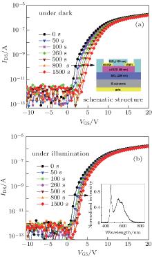
The inverted staggered a-IGZO TFT device studied in this work is fabricated on a heavily doped n-type silicon substrate, which also serves as a back gate electrode. Firstly, a 200-nm SiO2 gate insulator is deposited on the front side of silicon substrate by plasma-enhanced chemical vapor deposition (PECVD) at 350 ° C. A 50-nm a-IGZO layer is subsequently deposited on the SiO2 layer by direct-current magnetron sputtering at room temperature. The composition of the IGZO target used is In2O3:Ga2O3:ZnO = 1:1:1 mol% and the sputtering process is carried out in (Ar + O2) mixed gas with an O2/(Ar + O2) gas flow ratio of 15%. The deposited a-IGZO film is highly transparent to visible light, showing an average transmittance of over 95% in a wavelength range from 400 nm to 700 nm based on optical absorption measurement (not shown here). Optical photolithography and wet chemical etching are then adopted to pattern the a-IGZO active layer. Next, the source and drain Ti/Au (30 nm/70 nm) bi-layer electrodes are deposited by electron-beam evaporation and patterned by a lift-off process, resulting in an effective channel width/length (W/L) of 700 nm/70 nm. Finally, the devices are passivated by 100-nm PECVD SiO2 layer and are annealed in air at 250 ° C for one hour. The passivation layer should be enough to exclude the ambient effect, such as oxygen or water molecule absorption/desorption.[10– 12] A schematic cross-sectional diagram of the device structure is shown in the inset of Fig. 1(a).
During the reliability test, a-IGZO TFT is stressed and characterized with a Keithley 2612B sourcemeter at room temperature. The illumination is provided by a white light emitting diode (LED), which emits visible sub-bandgap energy light over a wide spectrum range. The typical emission spectrum of the white LED is shown in the inset of Fig. 1(b), which exhibits two main characteristic peaks in blue and yellow wavelength regions, respectively. The incident optical power is ∼ 0.1 mW/cm2.
Figure 1(a) shows the I– V transfer curves of a-IGZO TFT stressed as a function of time. During the positive gate bias stress, the gate bias of the TFT is kept at 20 V while both the source and drain contact electrodes are grounded. It is clear that the whole transfer curves shift towards positive direction after the a-IGZO TFT has been stressed, which is commonly explained by bias-induced carrier trapping at the channel/dielectric interface.[10] The a-IGZO TFT is also stressed under white light illumination. Figure 1(b) shows the corresponding transfer curves measured as a function of stress time. Similar positive shifts of the transfer curves are observed, while the amount of positive shift is apparently smaller.
The threshold voltage (Vt) of the transfer curve can be estimated based on linear extrapolation and is described as[11]

where μ FE and Cox are field effect mobility and dielectric capacitance per unit area, respectively. The μ FE can be further retrieved from the maximum transconductance gm= ∂ VDS/∂ VGS as

The calculated Vt as a function of stress time are shown in Figs. 2(a) and 2(b), respectively. It is found that the Vt shift varies rapidly at early stress time and then tends to be saturated at longer stress time. After 1500-s stress, the amount of Vt shift is ∼ 1.62 V when the device is under simply positive gate-bias stress (PBS), compared with ∼ 1.16 V when the device is under positive gate-bias illumination stress (PBIS). Here it should be noted that the white light used in this work has sub-bandgap photon energy. Thus, excitations of electron and hole pairs should be negligible, which is evidenced from the little increase of off-state leakage current of the TFT under PBIS. Since the effect of illumination is to reduce the Vt shift, one explanation is that the sub-bandgap white light could excite the trapped carriers at the channel/dielectric interface up to the conduction band, which works contrarily to the effect of bias-induced interface trapping.[12] Meanwhile, corresponding variations of field effect mobility are also observed. As shown in Fig. 2(b), when Vt shifts to higher values, with an original value of ∼ 11 cm2/V· s drops simultaneously. After PBS and PBIS, the decrements of drop are 1.44 cm2/V· s and 1.15 cm2/V· s, respectively. That is, the smaller the Vt shift, the less degradation there is. The degradation of μ FE can be explained by the enhanced interface scattering, as trapped electrons are strong electrostatic scattering centers.[13, 14] Since illumination could release some trapped electrons, the drop under PBIS condition is reduced.
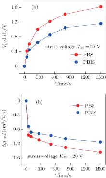 | Fig. 2. (a) Evolutions of Vt shift with time under PBS and PBIS. (b) The evolutions of field effect mobility μ FE with time under PBS and PBIS. |
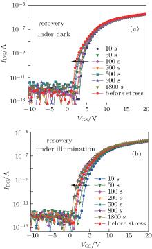 | Fig. 3. Transfer curves of the a-IGZO TFT measured as a function of time during the dark recovery (a) and the illumination recovery (b). |
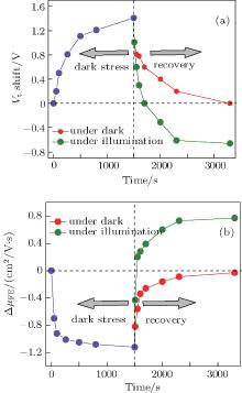 | Fig. 4. Time dependences of the Vt shift (a) and μ FE (b) under PBS and under the dark recovery and the illumination recovery. |
To further understand the illumination-induced electrical instability, the recovery processes of the a-IGZO TFT after PBS are studied under dark and under similar illumination condition as used for the PBIS measurement. In this test, the a-IGZO TFT is first stressed at a gate bias of 20 V under dark recovery for 1500 s so as to fill the interface states with a large number of electrons. Then, the device is kept under dark recovery or under prolonged white light illumination. The transfer curves are measured at selected time in the recovery process. As shown in Fig. 3, under both dark and illuminated conditions, the transfer curves of the TFT under recovery would shift towards negative direction, which can be explained by the gradual release of trapped electrons from interface states.[15] However, the amount of back-shift for the device recovered under illumination is apparently larger than that of the device recovered under dark. Figure 4(a) shows the detailed Vt shift as a function of time. After 3000 s, the Vt of the device recovered under dark almost returns to its original value before the PBS and tends to be saturated, suggesting that nearly all of the PBS-induced trapped electrons are released. On the other hand, as shown in Fig. 4(a), when the device is recovered under illumination, the Vt shifts back apparently faster. This observation agrees with the suggested photon-assisted detrapping mechanism. Interestingly, in this case the Vt does not stop at its initial value but continues to shift towards negative direction, resulting in a saturated Δ Vt of − 0.7 V. In the recovery process, there is a simultaneous increase of μ FE in Fig. 4(b), which should be caused by the reduced interfacial scattering probability.[16] However, there is again an apparent difference between dark recovery and illumination recovery. The μ FE of the device recovered under dark conditions would eventually return to its initial value before the PBS, while the device recovered under illumination would exhibit an even higher saturated μ FE.
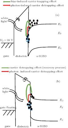
To explain the unusual recovery behavior of the a-IGZO TFT under illumination, a physical picture is further suggested. It is believed that under equilibrium there are already some trapped electrons existing in the interfacial region, which fills up with all the interface states below the Fermi level as well as part of the band-tail states. Part of these originally trapped electrons can also be excited by the sub-bandgap illumination. Thus, towards the end of the illumination recovery, the number of interfacial electrons as well as the relevant scattering centers can be even lower than those in the initial equilibrium state, leading to a reduced Vt and an enhanced μ FE. The energy band diagrams illustrating the suggested carrier trapping and detrapping mechanisms during the PBIS and the recovery process are shown in Fig. 5.
Here it should be noted that there is another possible explanation for the unusual Vt recovery behavior under illumination. It is reported that singly ionized oxygen vacancies (Vo+ ) and double ionized oxygen vacancies (Vo2+ ) within the a-IGZO active layer can be induced by sub-bandgap energy photons, which would release electrons onto the conduction band.[17] An extra number of electrons would cause the reduction of Vt and the μ FE could increase due to the enhanced perlocation conduction mechanism. In addition, the generation of ionized oxygen vacancies is accompanied by new trap state formation, which would degrade the sub-threshold swing (SS) of the TFTs.[18– 22] Based on a separate negative bias illumination stress (NBIS) study, such an effect does occur in the fabricated a-IGZO TFT, which would cause apparent negative Vt and sub-threshold swing (SS) degradation (not shown here). However, the influence of photo-excitation of oxygen vacancies should be weak in the present study because there is nearly no SS degradation in the PBIS process and the fairly small SS degradation during the illumination recovery (see Figs. 1(b) and 3(b)). It is believed that when the TFT is stressed by positive gate bias or with gate floating, the photo-induced positively charged oxygen vacancies near the channel/dielectric interface can be effectively neutralized by accumulated electrons or free electrons. A detailed discussion and experimental evidence for this explanation will be reported in another paper.
In this paper, the influence of white light illumination on the electrical stability of a-IGZO TFTs is studied when the devices are stressed by positive gate-bias and in the recovery process. Under prolonged positive gate bias stress, the device illuminated by white light exhibits smaller positive threshold voltage shift and less field-effect mobility degradation than those of the device stressed under dark condition. Such an observation is explained by a competition between bias-induced interface carrier trapping and photon-induced carrier detrapping effects. It is further found that white light illumination could cause a faster recovery process and could also excite trapped carriers originally exiting at the device interface, leading to an even lower threshold voltage and a higher field-effect mobility than those in an equilibrium state.
| 1 |
|
| 2 |
|
| 3 |
|
| 4 |
|
| 5 |
|
| 6 |
|
| 7 |
|
| 8 |
|
| 9 |
|
| 10 |
|
| 11 |
|
| 12 |
|
| 13 |
|
| 14 |
|
| 15 |
|
| 16 |
|
| 17 |
|
| 18 |
|
| 19 |
|
| 20 |
|
| 21 |
|
| 22 |
|


