†Corresponding author. E-mail: hubo2011@semi.ac.cn
Based on semiclassical Boltzamnn transport theory in random phase approximation, we develop a theoretical model to investigate low-temperature carrier transport properties in relatively high doped bilayer graphene. In the presence of both electron–hole puddles and band gap induced by charged impurities, we calculate low-temperature charged impurity scattering-limited conductivity in relatively high doped bilayer graphene. Our calculated conductivity results are in excellent agreement with published experimental data in all compensated gate voltage regime of study by using potential fluctuation parameter as only one free fitting parameter, indicating that both electron–hole puddles and band gap induced by charged impurities play an important role in carrier transport. More importantly, we also find that the conductivity not only depends strongly on the total charged impurity density, but also on the top layer charged impurity density, which is different from that obtained by neglecting the opening of band gap, especially for bilayer graphene with high top layer charged impurity density.
Since its tunable band gap, bilayer graphene (BLG) has been a subject of intense research for both scientific interest and technological purpose.[1– 4] In different experiments, the net carrier density-dependent BLG conductivity behavior has been revealed on low-field transport measurements.[5, 6] It is widely accepted that short-range scattering[7– 9] and charged impurity scattering[3] are the significant factors in limiting the BLG conductivity or mobility at low temperature, where phonon scattering can be strongly suppressed. However, short-range scattering should be more pronounced in CVD-grown or SiC-derived graphene.[10, 11] On doped mechanically exfoliated BLG considered in our work, STM studies have revealed that the short-range defect density is negligibly small compared to charged impurity density.[12] The charged impurity scattering of BLG has been theoretically considered in parabolic dispersion approximation for the BLG Hamiltonian and has been suggested to be the dominant source of scattering in explaining the experimental data observed by different groups.[13] For all we know, low-energy parabolic dispersion for a low doped BLG is a good approximation in low net carrier density regime.[14] However, for a relatively high doped BLG, charged impurities are responsible not only for the formation of electron– hole puddles, [15, 16] but also for the opening of band gap.[17– 20] Recent experimental studies have investigated low-temperature charged impurity scattering-limited conductivity behavior by depositing potassium on BLG to understand the effect of charged impurity-induced disorder in relatively high doped BLG.[21] It is shown that the product of the carrier mobility and the total charged impurity density is not as constant as predicted for different relatively high net carrier densities. This somewhat derivation is in contradiction with the theoretical model in the parabolic approximation, indicating that the opening of charged-impurity-induced band gap should also be theoretically treated to understand carrier conductivity behavior in relatively high doped BLG.
The goal of our work is to develop a detailed microscopic transport theory to investigate charged impurity scattering-limited conductivity in relatively high doped BLG by considering the opening of band gap at low temperature. In addition, an analytic statistical model is also included to understand electron– hole puddles induced by charged impurities. It must be pointed out that the puddles potential fluctuation is assumed to affect an equilibrium Fermi distribution function in our presented model, rather than the overall density of state in BLG, which can also provide a possible explanation for low-temperature finite conductivity characteristic around the charge-neutrality point.
In this section, we consider a relatively high doped Bernal-stacking BLG supported on SiO2 substrate. In the presence of band gap induced by both charged impurities and gate voltage, the effective low-energy two-band Hamiltonian can be well approximated by expanding its minimal tight-binding spectrum near the K point[14]

where 


with

where L2 is the area of the system, θ k = arctan(ky/kx) is the polar angle of the wave vector k, and tan α k= ℏ 2k2/(2m*U). Its finite band gap is 2|U|, and density of state (DOS) per unit energy is 
Next, we account for electron– hole puddles of BLG due to the existence of charged impurities. To avoid the complication, we adopt a simplified but physical assumption for the puddles potential V, which can be approximated as an uniform distribution function in the range from − Δ to Δ . This is similar to previous studies, [6, 22] in which the puddle fluctuation potential can be approximated as a periodic step or Gaussian distribution function. At finite temperature, an equivalent equilibrium distribution function in the presence of electron– hole puddles can be obtained by

where μ is the average Fermi level, β = 1/kT, and Δ is the potential fluctuation parameter, which is used as an adjustable parameter. At zero temperature, f(ε )= (ϑ (μ + Δ − ε )− ϑ (μ − Δ − ε ))/2Δ . Note that when Δ = 0, it reduces to Fermi distribution function f(ε )= { 1+ exp[β (ε − μ )]} − 1.
From Gauss’ s law, the net carrier densities (nt, b) on the layers can be obtained by

where 


with

where the plus (minus) sign corresponds to the top (bottom) layer, 

At low temperature, phonon scattering is strongly suppressed, long-range screening Coulomb scattering dominates low-field carrier conductivity since short-range disorder scattering may be not a significant factor in doped mechanically exfoliated BLG, where an estimated defect density is negligibly small relative to charged impurity density. Therefore, a Boltzmann transport theory in the random phase approximation (RPA) is used to calculate the low-temperature conductivity by considering only long-range charged impurity scattering as the main scattering mechanism. The carrier conductivity is the sum of electron and hole conductivities, given by

where τ (ε ) is the energy-dependent momentum relaxation time. According to the Fermi golden rule, it is obtained by

with 

where θ kk′ is the scattering angle between k and k′ , υ (q)= e2/(2κ q) is the Fourier transform of two-dimensional (2D) Coulomb scattering potential between an electron and an impurity, where κ is the effective background dielectric constant of BLG. In Eq. (9), ε (q) is the 2D finite temperature static RPA dielectric (screening) function of BLG, obtained by

where Π (q, T) is the BLG irreducible finite-temperature polarizability function, which is given by

with

where k′ = k+ q. After performing the summation over ss′ , we can decompose the polarizability into two parts as

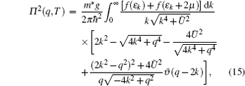
where Π 1(q) is the virtual interband polarizability due to the transition from the valence band electron into conduction band, and Π 2(q, T) is the sum of the temperature-dependent intraband and interband polarizabilities. The sum over k in Eq. (11) can be converted to an integral. By setting 

and

where 

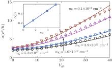
Using the model described above, we calculate charged impurity scattering-limited low temperature conductivity of doped BLG on SiO2 substrate. To facilitate comparison quantitatively with experiment from Ref. [21], we also introduce an initial total charged impurity density nd, 0 = 3.5 × 1012 cm− 2 and the top layer charged impurity density ndt, 0 = 0.3 × 1012 cm− 2 so that the total impurity density is nd= nd, 0+ nK, and the top layer impurity density is ndt= ndt, 0+ nK, where nK is the potassium concentration deposited on the top layer of BLG. It should be noted that an initial charged impurity may include the acceptor and donor charged impurity. Figure 1 shows the experimental (symbols) and calculated (lines) conductivity σ as a function of Vg0 for different nK= 0.1, 1.6, 3.9, 5.3× 1012 cm− 2 at T= 10 K. The inset gives the corresponding fitting value of the potential fluctuation parameter (Δ = 0.13γ , 0.26γ , 0.46γ , 0.59γ ) for different nK. By considering such an appropriate potential fluctuation parameter, our calculated conductivities can agree well with the experimental conductivities for different nK at T= 10 K. It is found that Δ increases nearly linearly with increasing nK in the range of nK we studied, reflects the variance of electron– hole puddles induced by different nd and ndt, which can be well estimated experimentally by scanning tunneling spectroscopy measurement.[9, 10] It is worthwhile to note that the total carrier density is relatively high in the whole compensated gate voltage regime considered, even at the charge-neutrality point. For instance, our calculated total carrier densities for different nK are estimated to be the order of magnitude of 1012 cm− 2 around the charge-neutrality point (Vg0= 0), which are consistent with the experimental results from Hall measurement on BLG, in which measured low-temperature total carrier density is ∼ 1.5× 1012 cm− 2 at the charge-neutrality point.[6] This indicates that random phase approximation may also be valid in low compensated gate voltage regime. In addition, it should also be pointed out that in our disorder model, the conductivity is always finite at much lower temperatures and net carrier densities, which is different from localization model, where the conductivity is zero at T= 0.[23]
 | Fig. 1. Calculated conductivity σ as a function of (Vg0) for different nK= 0.1, 1.6, 3.9, 5.3× 1012 cm− 2 at T= 10 K (lines) and comparison with experimental data from Ref. [21] (symbols). The inset gives the corresponding fitting value of Δ used in the conductivity calculations for different nK. |
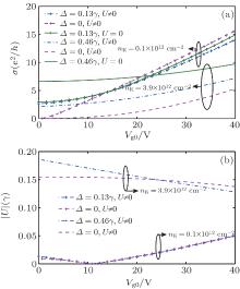
To obtain a full view of the role of both band gap and electron– hole puddles induced by charged impurities, we calculate carrier conductivity σ and the corresponding interlayer asymmetry | U| for different nK= 0.1, 3.9× 1012 cm− 2 at T= 10 K, as shown in Fig. 2. For comparison the results obtained by neglecting either charged impurity-induced band gap or electron– hole puddles are also shown. For the case of low nK= 0.1× 1012 cm− 2, the effect of electron– hole puddles induced by charged impurities on carrier conductivity begins to be obviously weaken as Vg0 increases, however, when compensated gate voltage is high up to ∼ 13 V, the inclusion of electron– hole puddles induced by charged impurities will never change much. In addition, the effect of band gap induced by charged impurities on carrier conductivity is insignificant due to disorder-induced negligibly small band gap, as shown in Fig. 2(b). This shows that parabolic dispersion approximation gives a good approximation for BLG with low nK. For the case of relatively high nK= 3.9× 1012 cm− 2, the effect of electron– hole puddles induced by charged impurities on carrier conductivity starts to be noticeable for lower values of Vg0, even though the effect of electron– hole puddles induced by charged impurities is also decreasing, especially at relatively high Vg0. If band gap induced by charged impurities is not considered, the calculated conductivity is overestimated in the whole range of compensated gate voltage regime considered, which comes from the fact that large band gap can be produced in the whole range of compensated gate voltage regime considered, and results in the decrease of carrier conductivity. For instance, when Vg0= 0, it can be overestimated as much as a factor of ∼ 3 due to large band gap 120 meV.
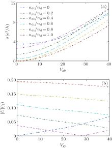
To further understand the role of the top layer-charged impurity, we investigate the low-temperature BLG conductivity behavior for different ndt. The total charged impurity density and the potential fluctuation parameter used in our conductivity calculations are set to be 5.0× 1012 cm− 2 and 0.20γ , respectively. Figure 3 shows that the calculated conductivity σ and the corresponding | U| as a function of Vg0 for different scaled ndt/nd= 0∼ 1.0 at T= 10 K. From Fig. 3(a), we can see that the calculated conductivity increases with decreasing scaled ndt/nd in low compensated gate voltage regime, however, it shows a non-monotonic conductivity behavior in high compensated gate voltage regime. This conductivity behavior is attributed to the corresponding non-monotonic charged impurity-induced band gap, as shown in Fig. 3(b). It shows that our calculated conductivity not only depends strongly on nd, but also strongly on ndt, which can provide a possible explanation for why the product of the carrier mobility and the total charged impurity density is not as constant as predicted for different relatively high net carrier densities.[21]
In conclusion, we have developed a detailed microscopic transport theory to investigate charged impurity scattering-limited conductivity in relatively high doped BLG at low temperature. In the presence of both electron– hole puddles and band gap induced by charged impurities, we calculated low-temperature charged impurity scattering-limited conductivity. Our calculated conductivity characteristics show very good agreement with experimental results by using potential fluctuation parameter as only one free fitting parameter, indicating both electron– hole puddles and band gap induced by charged impurities play an important role in carrier transport of relatively high doped BLG. More importantly, we also find that the carrier conductivity has a strong dependence not only on the total charged impurity density but also on the top layer charged impurity density in the whole range of compensated gate voltage regime considered, which is different from that obtained by neglecting charged-impurity-induced band gap, especially for doped BLG with high top layer charged impurity density.
| 1 |
|
| 2 |
|
| 3 |
|
| 4 |
|
| 5 |
|
| 6 |
|
| 7 |
|
| 8 |
|
| 9 |
|
| 10 |
|
| 11 |
|
| 12 |
|
| 13 |
|
| 14 |
|
| 15 |
|
| 16 |
|
| 17 |
|
| 18 |
|
| 19 |
|
| 20 |
|
| 21 |
|
| 22 |
|
| 23 |
|


