Jiangsu Provincial Key Laboratory of Advanced Photonic and Electronic Materials, and School of Electronic Science and Engineering, Nanjing University, Nanjing 210093, China
Collaborative Innovation Center of Advanced Microstructures, Nanjing University, Nanjing 210093, China
Peter Grünberg Research Center, Nanjing University of Posts and Telecommunications, Nanjing 210003, China
*Project supported by the National Basic Research Program of China (Grant Nos. 2011CB301900 and 2011CB922100) and the Priority Academic Program Development of Jiangsu Higher Education Institutions, China
Abstract
The time and temperature dependence of threshold voltage shift under positive-bias stress (PBS) and the following recovery process are investigated in amorphous indium-gallium-zinc-oxide (a-IGZO) thin-film transistors. It is found that the time dependence of threshold voltage shift can be well described by a stretched exponential equation in which the time constant τ is found to be temperature dependent. Based on Arrhenius plots, an average effective energy barrier E τstress = 0.72 eV for the PBS process and an average effective energy barrier E τrecovery = 0.58 eV for the recovery process are extracted respectively. A charge trapping/detrapping model is used to explain the threshold voltage shift in both the PBS and the recovery process. The influence of gate bias stress on transistor performance is one of the most critical issues for practical device development.
Recently, thin-film transistors (TFTs) based on amorphous oxide semiconductors have received a great deal of interest as a potential backplane technology for next generation display applications. In particular, amorphous indium-gallium-zinc-oxide (a-IGZO), first proposed by Hosono et al. in 2004[1] and intensively developed across the world ever since, [2– 7] is regarded as the most promising oxide material for making TFT channels. Compared with traditional semiconductors such as amorphous silicon (a-Si) and recently developed organic channel materials, a-IGZO has shown readily apparent advantages including high electron mobility, good uniformity, low processing temperature and high optical transparency to visible light.[1, 8]
For practical TFT applications, instability suffering from conditions such as gate-bias stress and visible-light illumination must be minimized. Although there have been some reports on the instability behaviors of a-IGZO TFTs, [9– 12] the underlying mechanisms responsible for electrical instability, which are likely strongly dependent on detailed processing parameters, are still controversial. In the present work, the effect of positive-bias stress (PBS) on threshold voltage instabilities of a-IGZO TFTs as well as the following recovery behavior when the devices are left unbiased are studied as a function of time. The threshold voltage shift occurring in both the PBS and the recovery process is found to be strongly temperature dependent. The corresponding effective energy barriers are extracted and compared with the related data in the literature. The experimental results support a conclusion that charge trapping/detrapping between the gate insulator and the a-IGZO channel is the major mechanism for PBS instability.
2. Experiment
The a-IGZO TFTs tested in this work are fabricated on heavily doped n-type silicon substrate, which serves as the back gate. A 200-nm SiO2 gate insulator layer is first deposited on the wafer’ s front side by plasma enhanced chemical vapor deposition at 300 ° C. A 50-nm a-IGZO active layer is then deposited by dc sputtering at room temperature. The ceramic IGZO target used is composed of In2O3:Ga2O3:ZnO = 1:1:1 in mole ratio and the oxygen content of the Ar+ O2 mixture gas is maintained at 15% during sputtering. Afterward, the active region is defined by photolithography and wet chemical etching. Next, a Ti/Au (30 nm/70 nm) bi-layer is deposited by e-beam evaporation and patterned as the source/drain contact electrodes. The effective channel region is formed as 100-μ m in width and 20-μ m in length. Finally, all device samples are subjected to thermal annealing at 300 ° C in air for 1 h.
To study the electrical instability behaviors of a-IGZO TFTs, the influence of PBS on threshold voltage shift and the following recovery process after PBS are examined as a function of time. Positive gate bias stress of 30 V is applied with both the source and the drain electrodes of the TFT grounded. At selected times, the bias stress is interrupted and the transfer characteristics of the TFT are quickly measured with VDS = 0.1 V. All electrical stress and I– V measurements are conducted in darkness by using a Keithley 2612 SourceMeter. The recovery process is monitored by measuring the transfer curves at fixed times after 3000 s PBS at 30 V. To further investigate the temperature dependent electrical instability, the same measurements are repeated at different ambient temperatures ranging from 30 ° C to 90 ° C.
3. Results and discussion
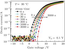
Figure 1 shows the evolution of transfer curves of the a-IGZO TFT as a function of PBS time. The curves continuously shift in the positive direction. After 3000 s PBS, the amount of threshold voltage shift reaches about 3.58 V. Here the threshold voltage (Vth) of the TFT is defined as the gate voltage (VGS) value where the drain current (IDS) rises to 10 nA in a transfer curve. In spite of the large threshold voltage shift (Δ Vth), the subthreshold swing (SS) of the TFT remains almost constant at about 0.58± 0.07 V/dec, while there is also no apparent variation of field-effect mobility (μ FE) with a nearly constant value of ∼ 10.5± 0.6 cm2· V− 1· s− 1.
Fig. 1. Transfer characteristics of the a-IGZO TFT under PBS stress as a function of stress time.
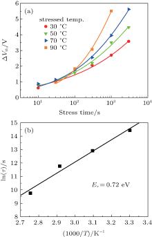
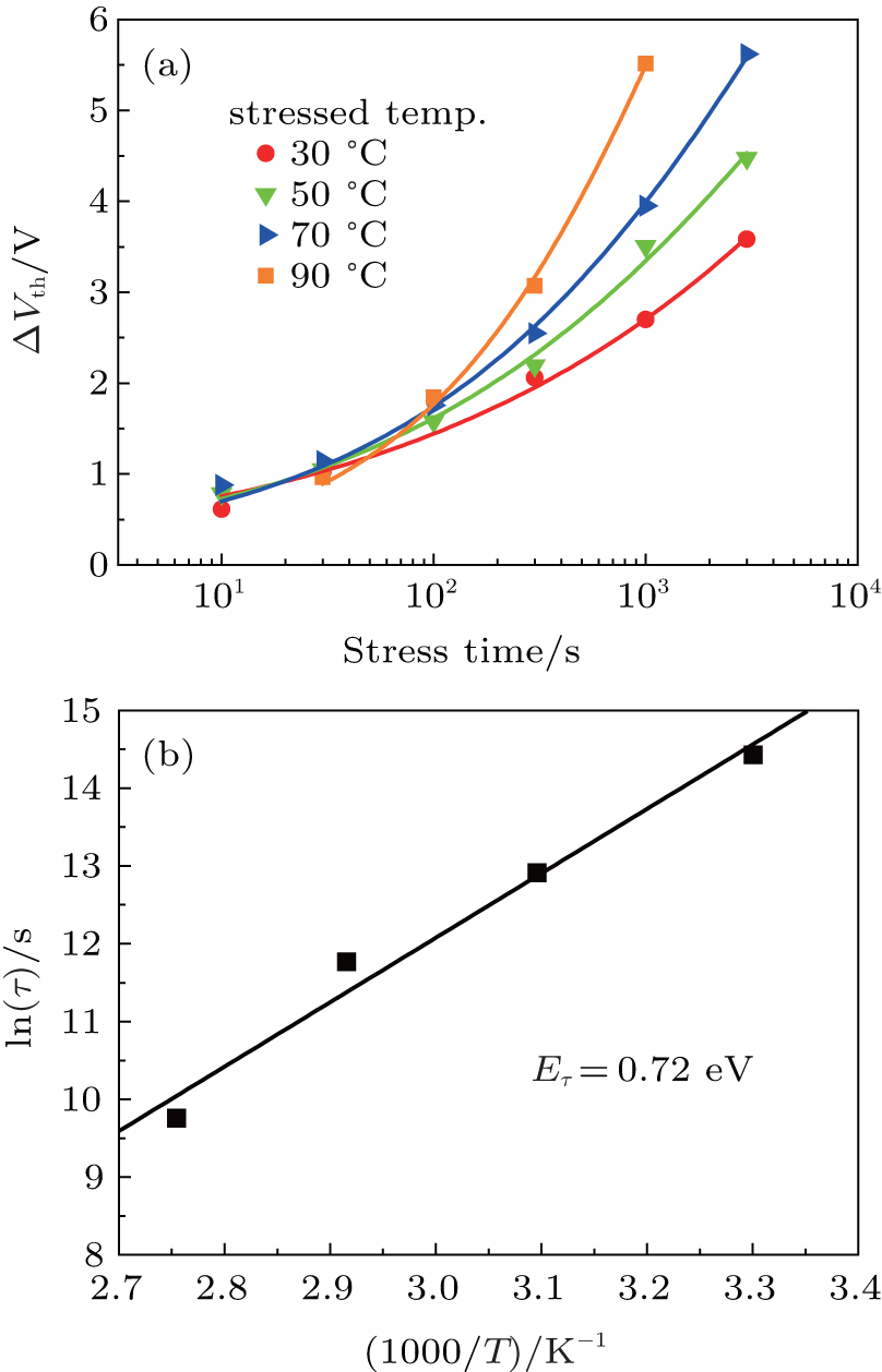
The amount of Δ Vth as a function of time measured at various temperatures is shown in Fig. 2(a). It is found that the time dependence of Δ Vth can be fitted with a stretched-exponential equation[9]
where τ denotes a time constant, β is a stretched-exponential exponent, and Δ Vtho is the Δ Vth at infinite stressing time. The fitting curves are also shown (solid) in Fig. 2(a). Through numerical fitting, a value of 1.8 × 10⁶ s for τ at 303 K is deduced. It is further found that τ is strongly temperature dependent and decreases at higher temperatures, indicating that the stress-induced instability behavior is thermally activated.
Fig. 2. (a) Time dependence of Vth shift at different stress temperatures. The measured data are well fitted with a stretched-exponential equation. (b) Stress time constant lnτ as a function of reciprocal temperature.
Figure 2(b) shows the evolution of lnτ as a function of reciprocal temperature. As it is a typical thermally activated process, the data points can be linearly fitted by using the following equation:[9]
where Eτ is the average effective energy barrier, τ 0 is a prefactor, T is the absolute temperature and kB is the Boltzmann constant. The good linear dependency of the data points indicates that the thermally activated process is governed by a consistent effective energy barrier Eτ . An Eτ of ∼ 0.72 eV is derived for the PBS process, which must be related to the microscopic nature of the trap sites.
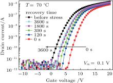
In applications such as active matrix displays, the TFT would be switched on and off occasionally. The generated Vth shift by PBS relaxes in the off-state. Thus, the recovery behavior after stress is also important for investigation. Figure 3 shows the recovery behavior of the TFT at 70 ° C after 3000 s PBS at 30 V. It is clear that the transfer curves shift negatively toward the initial state while their subthreshold slopes remain almost the same.
Fig. 3. Transfer characteristics of the a-IGZO TFT at 70 ° C as a function of recovery time after 3000 s PBS at 30 V.
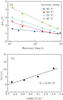
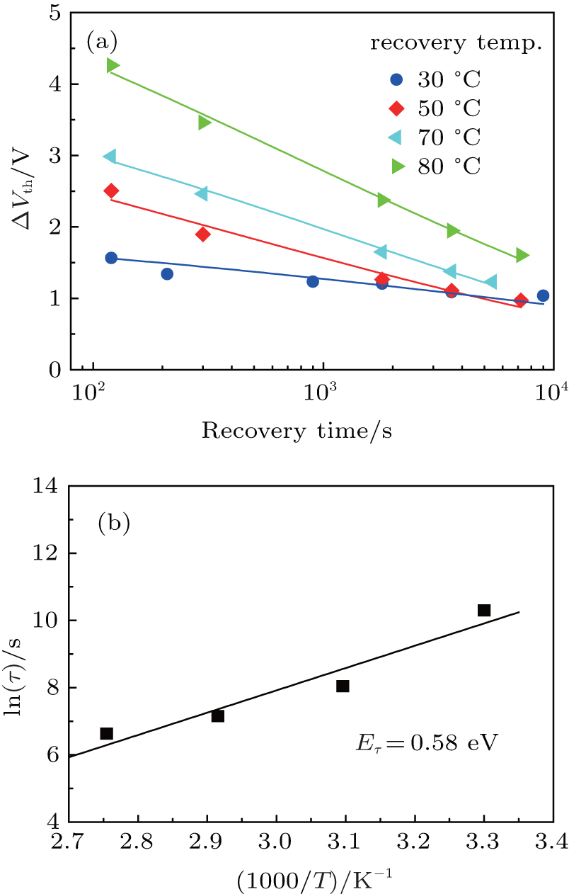
Figure 4(a) shows the time dependence of the Vth shift during the recovery process at various temperatures. Still, the data can be fitted with the stretched-exponential equation
where Δ Vth_max is the Δ Vth right before the relaxation begins. A value of 3.0 × 10⁴ s for time constant τ at 303 K is derived, which is two orders of magnitude smaller than the time constant for the PBS process. Based on an Arrhenius plot and numerical fitting similar to that shown in Fig. 4(b), an average effective energy barrier Eτ of 0.58 eV is calculated for the recovery process, which is smaller than the effective energy barrier of the PBS process, indicating the recovery process is less temperature sensitive.
Fig. 4. (a) Time dependence of Vth shift at different recovery temperatures. The measured data are well fitted with a stretched-exponential equation. (b) Recovery time constant lnτ as a function of reciprocal temperature.
Previous studies on oxide semiconductor TFTs have concluded that there are two main mechanisms responsible for electrical instability.[13– 16] One is carrier trapping at defect states, and the other is point defect generation, which would consequently change the subthreshold swing.[15, 16] In the present case, there is no apparent change of SS and μ FE, indicating that during the PBS and the following recovery process, creation of additional defect states is negligible. Thus, the PBS-induced Vth shift must be caused by the trapping of electrons at the existing interfacial trapping states, which partially screens the applied gate bias and makes the effective gate voltage smaller. As the electron trapping process is reversible, it can be easily understood that the recovery of the transfer curves without gate bias stress must be due to electron detrapping from interfacial states.
Based on the above, the carrier trapping mechanisms under PBS stress can be described as follows: under high positive gate bias, the Fermi level along the device channel moves above the mobility edge, and carriers within a-IGZO channel accumulate at the semiconductor/gate insulator interface.[17] As temperature increases, the Fermi level moves up further due to the enhanced dopant ionization effect and meanwhile, more carriers are thermally activated above the Fermi level. As a result, the rate for carriers to overcome the effective energy barrier and to be trapped at the interfacial states is enhanced, leading to a decreased characteristic time constant τ at higher temperatures.
The time constants and activation energies extracted in this work are summarized in Table 1 along with similar parameters reported in the literature. Compared with the past reports, the device fabricated in this work features larger time constants and higher activation energies of electrical instability in both the PBS and the recovery process. The relatively better device stability is likely caused by the application of a slightly higher oxygen partial pressure of O2/(O2+ Ar) = 15% during the a-IGZO deposition process. The high oxygen partial pressure during sputtering deposition usually enables the a-IGZO film to have a lower concentration of oxygen vacancies and possibly better interface quality. Further comparative reliability study of a-IGZO TFTs deposited and annealed at different oxygen partial pressures will be conducted in future work. Here it should be noted that the overall time constants of the performance shift of a-IGZO TFTs are still much smaller than those of a-Si:H and microcrystalline Si TFTs (see Table 1), indicating that the interface quality of the current a-IGZO TFTs is still poor and has to be significantly improved.
Table 1.
Table 1.
Table 1. Summary of characteristic time constant Eτ and effective energy barrier Eτ of PBS-induced electrical instability for a-IGZO TFTs, as well as for Si-based TFTs. The key processing parameters of the a-IGZO TFTs are also listed.
Active layer/gate dielectric/post annealing in air
Note: the notation PO2 means the oxygen partial pressure during a-IGZO deposition.
grown by PECVD;
grown by thermal oxidation.
Table 1. Summary of characteristic time constant Eτ and effective energy barrier Eτ of PBS-induced electrical instability for a-IGZO TFTs, as well as for Si-based TFTs. The key processing parameters of the a-IGZO TFTs are also listed.
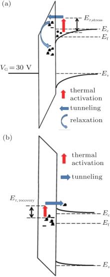
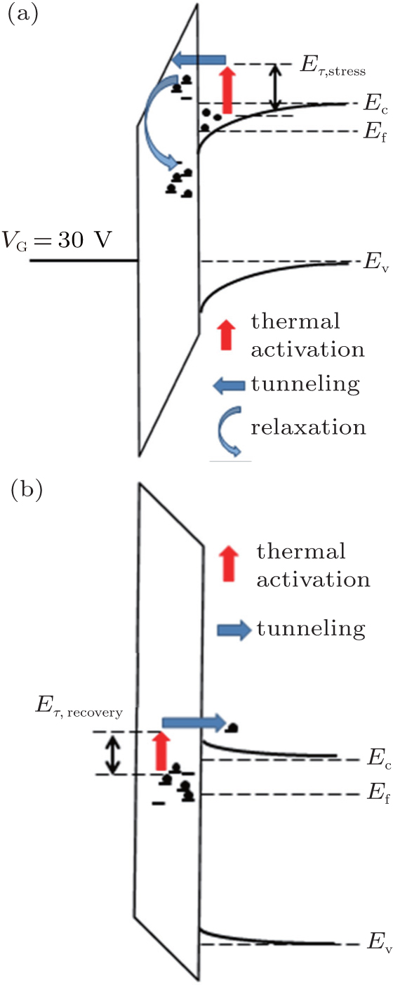
The corresponding schematic energy band diagrams of charge trapping and detrapping processes are presented in Fig. 5. Figure 5(a) shows that during the PBS process, electrons accumulate at the channel/dielectric interface. Then through thermionic-field emission, electrons need to overcome an average effective energy barrier of 0.72 eV to be injected into the trap states at the near interface of the gate insulator. In detail, the thermionic-field emission process must include thermal activation, subsequent tunneling and then possible relaxation to the lower energy interface states. Figure 5(b) shows that during the un-biased recovery process, the trapped electrons could be thermally activated and emitted back into a-IGZO channel. The extracted Eτ of 0.58 eV is the average effective energy barrier that the trapped electrons need to overcome.
Fig. 5. Schematic energy band diagram of (a) the stress process and (b) the recovery process. Here, Ec is the conduction band minimum, Ef is the Fermi level, and Ev is the valence band maximum.
4. Conclusion
In summary, the effect of positive gate bias stress on a-IGZO TFTs and the following recovery process are investigated as a function of time and at various temperatures. It is found that the time dependence of the Vth shift can be described by a stretched exponential equation. Effective energy barriers of 0.72 eV for the stress process and 0.58 eV for the recovery process are extracted. Interfacial carrier trapping and detrapping are confirmed as the major mechanisms for the threshold voltage shift during the PBS and the recovery process.
TripathiA K, SmitsE C P, van der PuttenJ B P H, van NeerM, MynyK, NagM, SteudelS, ViccaP, O’NeillK, van VeenendaalE, GenoeJ, HeremansP and GelinckG H2011Appl. Phys. Lett. 98162102DOI:10.1063/1.3579529[Cited within:1]
3
HuangX M, WuC F, LuH, RenF F, ChenD J, ZhangR and ZhengY D2013Appl. Phys. Lett. 102193505DOI:10.1063/1.4805354[Cited within:1]
LiX F, XinE L, ShiJ F, ChenL L, LiC Y and ZhangJ H2013Acta Phys. Sin. 62108503DOI:10.7498/aps.62.108503(in Chinese)[Cited within:1]
8
FortunatoE M C, BarquinhaP M C, PimentelA C M B G, GoncalvesA M F, MarquesA J S, PereiraL M N and MartinsR F P2005Adv. Mater. 17590DOI:10.1002/(ISSN)1521-4095[Cited within:1]
9
LeeJ M, ChoI T, LeeJ H and KwonH I2008Appl. Phys. Lett. 93093504DOI:10.1063/1.2977865[Cited within:3]
10
LopesM E, GomesH L, MedeirosM C R, BarquinhaP, PereiraL, FortunatoE, MartinsR and FerreiraI2009Appl. Phys. Lett. 95063502DOI:10.1063/1.3187532[Cited within:1]
11
ChenT C. , ChangT C, TsaiC T, HsiehT Y, ChenS C, LinC S, HungM C, TuC H, ChangJ J and ChenP L2010Appl. Phys. Lett. 97112104DOI:10.1063/1.3481676[Cited within:1]
12
ChowdhuryM D H, MiglioratoP and JangJ2011Appl. Phys. Lett. 98153511DOI:10.1063/1.3580611[Cited within:1]
... in 2004[1] and intensively developed across the world ever since,[2#cod#x2013 ...
... [1,8] ...
1
2011
0.0
0.0
... in 2004[1] and intensively developed across the world ever since,[2#cod#x2013 ...
1
2013
0.0
0.0
1
2014
0.0
0.0
1
2014
0.0
0.0
1
2012
0.0
0.0
1
2013
0.0
0.0
... 7] is regarded as the most promising oxide material for making TFT channels ...
1
2005
0.0
0.0
... [1,8] ...
3
2008
0.0
0.0
... Although there have been some reports on the instability behaviors of a-IGZO TFTs,[9#cod#x2013 ...
... Vth can be fitted with a stretched-exponential equation[9] ...
... As it is a typical thermally activated process, the data points can be linearly fitted by using the following equation:[9] ...
1
2009
0.0
0.0
1
2010
0.0
0.0
1
2011
0.0
0.0
... 12] the underlying mechanisms responsible for electrical instability, which are likely strongly dependent on detailed processing parameters, are still controversial ...
1
1983
0.0
0.0
... [13#cod#x2013 ...
1
1987
0.0
0.0
1
1987
0.0
0.0
... [15,16] In the present case, there is no apparent change of SS and #cod#x03BC ...
2
1993
0.0
0.0
... 16] One is carrier trapping at defect states, and the other is point defect generation, which would consequently change the subthreshold swing ...
... [15,16] In the present case, there is no apparent change of SS and #cod#x03BC ...
1
2013
0.0
0.0
... [17] As temperature increases, the Fermi level moves up further due to the enhanced dopant ionization effect and meanwhile, more carriers are thermally activated above the Fermi level ...
1
2009
0.0
0.0
1
1998
0.0
0.0
1
2001
0.0
0.0
Temperature-dependent bias-stress-induced electrical instability of amorphous indium-gallium-zinc-oxide thin-film transistors


 , Wu Chen-Fei