Temperature-dependent bias-stress-induced electrical instability of amorphous indium-gallium-zinc-oxide thin-film transistors

Temperature-dependent bias-stress-induced electrical instability of amorphous indium-gallium-zinc-oxide thin-film transistors |
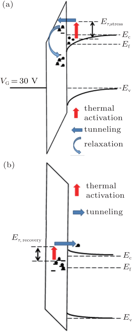
| Schematic energy band diagram of (a) the stress process and (b) the recovery process. Here, E c is the conduction band minimum, E f is the Fermi level, and E v is the valence band maximum. |
 |