


High performance trench MOS barrier Schottky diode with high- k gate oxide
[Zhai Dong-Yuana), b) , Zhu Junb) , Zhao Yi†a), c)  , Cai Yin-Fei
d) , Shi Yib) , Zheng You-Liaob) ]
, Cai Yin-Fei|
|


†Corresponding author. E-mail: yizhao@zju.edu.cn
*Project supported by the National Basic Research Program of China (Grant No. 2011CBA00607), the National Natural Science Foundation of China (Grant Nos. 61106089 and 61376097), and the Zhejiang Provincial Natural Science Foundation of China (Grant No. LR14F040001).
A novel trench MOS barrier Schottky diode (TMBS) device with a high- k material introduced into the gate insulator is reported, which is named high- k TMBS. By simulation with Medici, it is found that the high- k TMBS can have 19.8% lower leakage current while maintaining the same breakdown voltage and forward turn-on voltage compared with the conventional regular trench TMBS.
Until now, the main sources of energy have been coal, oil, and natural gas, the burning of which releases carbon dioxide into the atmosphere. With global awareness of the greenhouse effect, there is increasing demand for more efficient power electronic systems, because it is estimated that at least 50% of the electricity is controlled by power devices in widespread application fields, [1] such as high voltage electricity transmission, conventional domestic appliances with moderate voltage, and portable equipment with low voltage. Among all power electronic devices, the rectifier plays an important role. Compared with the most commonly used PN junction diode, the Schottky diode has the advantage of outstanding switching characteristics[2] which are essential for the miniaturization of electric devices.[3] But its large leakage current offsets this benefit in applications. In 1994, significantly enhanced performance was achieved by Mehrotra and Baliga by proposing a trench MOS barrier Schottky diode (TMBS).[4] Combining the charge coupling effect into a Schottky diode, TMBS significantly reduces the surface electric field intensity by changing the electric field distribution within the depletion region[5, 6] and consequently produces a lower leakage current compared with a planar Schottky diode with the same blocking voltage.
Worldwide, increasing concerns about environmental issues provide the motivation for the continuous improvement of the TMBS’ s performance. Since the emergence of the TMBS in 1997, there have been many research efforts for this purpose using the conventional regular trench TMBS as a benchmark. For example, researchers have proposed the filleted corner trench TMBS, ladder trench TMBS, [6] trapezoid mesa trench TMBS, [7] and so on. However, along with the improvement of any one of the three important parameters (blocking voltage, forward turn-on voltage, and leakage current), there are certain degradations of the other parameters.
In this study, we report a novel TMBS device, named high-k TMBS, which has a high-k material introduced into the gate insulator. By performing the simulation with Medici, [9] it is found that the high-k TMBS has a 19.8% lower leakage current while maintaining the same breakdown voltage of ∼ 51.8 V at the reverse current density of 10− 3 A/cm2 and the same forward turn-on voltage of ∼ 0.53 V at the current density of 150 A/cm2.
The structures of the conventional regular trench TMBS, which is a bench-mark of our study, and the high-k TMBS are schematically shown in Figs. 1(a) and 1(b), respectively.
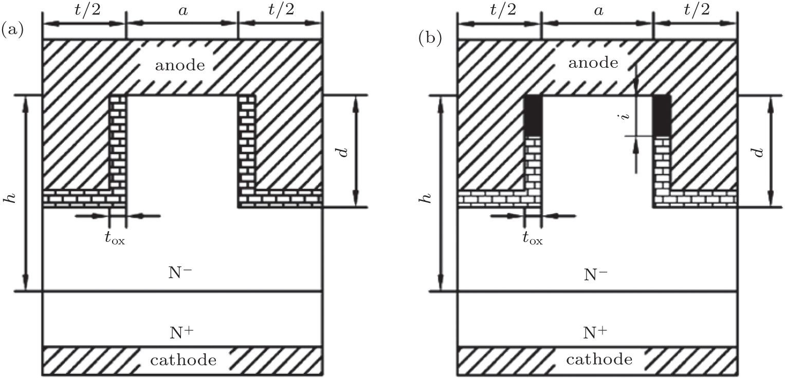 | Fig. 1. Schematics of (a) the conventional regular trench TMBS and (b) the high-k TMBS. |
In the following simulations, the basic parameters of these two structures have the same values as follows: the width between trenches (a) is 0.7 μ m, the trench width (t) is 0.7 μ m, the trench depth (d) is 1.65 μ m, the thickness of the gate isolator (tox) is 0.2 μ m, the thickness of the N− epi layer (h) is 4 μ m, and the doping concentration of the N− epi-layer is 2× 1016 cm− 3. The anode contact forms a Schottky contact with the N− epi-layer, while the cathode contact is ohmic.
The main difference of these two structures is that the gate insulator of the high-k TMBS is composed of two materials, one is the conventional SiO2, the other is the high-k material. As shown in Fig. 1(b), the height of the high-k insulator is designated as i.
In order to verify the superiority of the high-k TMBS compared with the conventional regular trench TMBS, Medici simulations have been performed on three kinds of TMBSs. The first is our proposed high-k TMBS, whose structure is shown in Fig. 1(b), where the height of the high-k (i) structure is 0.5 μ m. The second is the conventional regular trench TMBS with SiO2 as the gate insulator, named conventional SiO2 TMBS. The third is the conventional regular trench TMBS with HfO2 as the gate insulator, named conventional HfO2 TMBS. Figure 2 is the reverse I– V curves of the three aforementioned TMBSs. As can be seen from Fig. 2, the leakage current densities of the conventional SiO2 TMBS, the conventional HfO2 TMBS, and the high-k TMBS are 1.01× 10− 5 A/cm2, 1.2× 10− 5 A/cm2, and 8.1× 10− 6 A/cm2 (at − 40 V), respectively. The high-k TMBS has a leakage current density 19.8% lower than the conventional SiO2 TMBS. On the other hand, the breakdown voltages of these three TMBSs are 51.8 V, 45 V, and 51.74 V (at 10− 3 A/cm2), respectively. The breakdown voltage drop of the high-k TMBS compared with the conventional SiO2 TMBS is 0.06 V, which is negligible for real applications.
 | Fig. 2. Reverse I– V curves of the conventional SiO2 TMBS, the conventional HfO2 TMBS, and the high-k TMBS. |
From these values, we can conclude that the high-k TMBS has better reverse performance than the conventional regular trench TMBS, and the improvement cannot be achieved by simply changing the material of the gate insulator.
Figure 3 shows the forward I– V curves of the three TMBSs. The forward turn-on voltages of the conventional SiO2 TMBS, the conventional HfO2 TMBS, and the high-k TMBS are 0.530 V, 0.532 V, and 0.531 V (at turn-on current density of 150 A/cm2), respectively. The forward turn-on voltage of the high-k TMBS is larger than that of the conventional SiO2 TMBS by 0.28%. This is smaller than the deviation introduced by process variation, so it is negligible. Thus the high-k TMBS has the same forward performance as the conventional regular trench TMBS.
 | Fig. 3. Forward I– V curves of the conventional SiO2 TMBS, the conventional HfO2 TMBS, and the high-k TMBS. |
The facts above suggest that the structure of the high-k TMBS can significantly improve the electrical performance compared with the conventional regular trench TMBS, and the performance cannot be achieved just by changing the material of the gate insulator in the conventional regular trench TMBS.
We know that the electric field intensity distribution plays an important role in determining the breakdown voltage and the leakage current density. We plot the electric field intensity distributions along the trench edge of the three TMBSs in Fig. 4. We compare the electric field intensity distributions along the trench edge because the current flows along the trench edge, as shown in Fig. 4, when the avalanche breakdown happens.[10, 11]
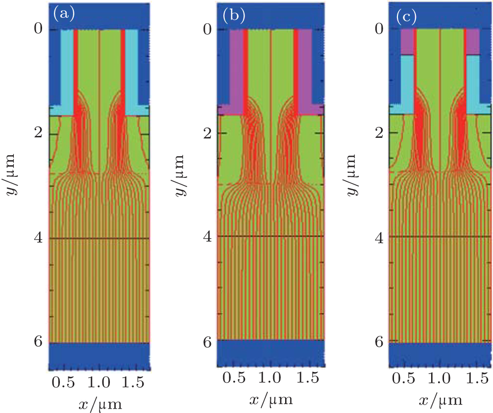 | Fig. 4. Current flow lines of (a) the conventional SiO2 TMBS, (b) the conventional HfO2 TMBS, and (c) the high-k TMBS after breakdown. |
From Fig. 5, we know that the surface electric field intensity of the high-k TMBS is much lower than that of the conventional SiO2 TMBS, which must result from the high dielectric constant of HfO2. So the leakage current of the high-k TMBS is lower than that of the conventional SiO2 TMBS. Meanwhile, the maximum electric field intensity in the depletion region is not increased, because the maximum field is located at the bottom of the insulator made by HfO2, as can be seen from Fig. 5. So the breakdown voltages of the high-k TMBS and the conventional SiO2 TMBS are almost the same. Finally, because the active area of the Schottky diode is of the same value in the three TMBSs, the forward turn-on voltages are close.
 | Fig. 5. Electric field intensity distributions of the conventional SiO2 TMBS, the conventional HfO2 TMBS, and the high-k TMBS at reverse voltage of 40 V. Inset shows the line 0.01 μ m away from the trench edge along which these electric field intensity distributions are plotted. |
We proposed a TMBS diode with a novel structure utilizing a high-k material constructing the upper part of the gate insulator in the trench. From the simulation results, it has been confirmed that the high-k TMBS can significantly improve the electrical performance compared with the conventional regular SiO2 TMBS. However, the performance cannot be achieved by only changing the insulator material, and better performance can be achieved if careful optimization is also done on the gate oxide structure.
| 1 |
|
| 2 |
|
| 3 |
|
| 4 |
|
| 5 |
|
| 6 |
|
| 7 |
|
| 8 |
|
| 9 |
|
| 10 |
|
| 11 |
|