

New method for fast morphological characterization of organic polycrystalline films by polarized optical microscopy*
[He Xiao-Chuana) , Yang Jian-Bingb) , Yan Dong-Hangb) , Weng Yu-Xiang†a)  ]
]
]
|
|


†Corresponding author. E-mail: yxweng@aphy.iphy.ac.cn
*Project supported by the National Natural Science Foundation of China (Grant No. 20933010) and the National Basic Research Program of China (Grant No. 2013CB834800).
A new method to visualize the large-scale crystal grain morphology of organic polycrystalline films is proposed. First, optical anisotropic transmittance images of polycrystalline zinc phthalocyanine (ZnPc) films vacuum deposited by weak epitaxial growth (WEG) method were acquired with polarized optical microscopy (POM). Then morphology properties including crystal grain size, distribution, relative orientation, and crystallinity were derived from these images by fitting with a transition dipole model. At last, atomic force microscopy (AFM) imaging was carried out to confirm the fitting and serve as absolute references. This method can be readily generalized to other organic polycrystalline films, thus providing an efficient way to access the large-scale morphologic properties of organic polycrystalline films, which may prove to be useful in industry as a film quality monitoring method.
As an alternative to inorganic electronics, organic electronics, bearing the advantages of low cost, light weight and flexibility, are under intensive scientific research and extensive industrial application.[1– 3] Organic electronics such as OLED, OFET, and OPV are based on organic semiconductors including small-molecule semiconductors and semiconducting polymers, which are usually vacuum-deposited, solvent-based coated or printed onto substrates as thin films.[4] The optical and electrical properties of the films including photoconductivity and carrier mobility are highly correlated to their morphological properties such as the molecular assembly pattern, crystal grain sizes, and crystallinity, [5, 6] and these properties directly determine the performance of the corresponding organic devices.[7, 8]
Since the device performance is so closely related to the film morphology, morphology checking is an essential step in the device fabrication process of the organic electronics industry. Morphological properties such as crystallinity, smoothness, boundary distribution, etc. need to be strictly monitored to certify uniformly high performance of these electronics. Methods such as AFM and TEM have already been used to obtain high-resolution morphologic images of organic films.[9, 10] However, these methods are not well suited for fast quantity applications, as they either work in scan mechanisms or depend on special preparation of samples. In this article we present a fast and simple all-optical method to obtain the large-scale crystal grain morphology of organic polycrystalline films. By combining POM imaging and a modeling based on the transition dipole approximation, the identification of the crystal grains and the visualization of the orientation and crystallinity of each crystal grain were demonstrated in a typical organic polycrystalline film, i.e., WEG ZnPc film. This method may meet the requirements of the morphology inspection in industrial device fabrication, where speed and quantity are of high priority.
ZnPc films were vacuum deposited by WEG, the detailed description of which can be found elsewhere.[9, 11] Briefly, at a vacuum of 10− 4– 10− 5 Pa, two monolayers (5-nm thick) of 2, 5-bis(4-biphenylyl)-bithiophene (BP2T) were thermally evaporated onto glass substrates, and then ZnPc was deposited onto the BP2T layer to 40-nm thickness. A 1-nm-thick F16CuPc was further deposited on the WEG ZnPc film as a buffer layer and a 60-nm thick Au was mask-deposited on the top as electrodes (the Au layer were prepared for electrical measurements that are not mentioned in this article).
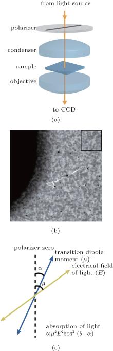
A simple POM technique was applied to obtain the anisotropic information of the films. In most applications, POM utilize two polarizers (commonly mentioned as one polarizer and one analyzer) to identify birefringent materials by enhancing the image contrast.[12, 13] However, here we focus only on the absorption anisotropy of the samples, so only one polarizer is equipped. In this way, the acquired images reflect only the intensity of the transmitted light without carrying any information of polarization, thus excluding any polarization effects present in the sample (such as birefringence). The schematic diagram of the optical path is shown in Fig. 1(a). A microscope (Nikon Eclipse Ti) is used with a halogen lamp as the source. A linear polarizer is positioned in front of the sample. By rotating the polarizer, linearly polarized light with different polarization angles is shone onto the sample. The transmitted light is collected by an objective (60x, NA: 0.75) and image onto a 2048× 2048 pixels CCD (Orca-flash 4.0, Hamamatsu). The spectrum of the light right
 | Fig. 1. (a) Schematic of the optical path of the POM measurement. (b) A full scale (222× 222 μ m) transmittance image under polarized light (see text for detail). (c) Demonstration of the light absorption through coupling between a transition dipole and an electrical field. |
before hitting the sample falls in the visible region almost exclusively between 500 and 800 nm, measured by an optical fiber spectrometer (HR4000CG-UV-NIR, Ocean optics).
The AFM images of the sample were acquired by an atomic force microscope (SPA400, Seiko instruments) with SiN probe using the contact mode.
To analyze the anisotropy information of the POM images, the absorption of polarized light features of the sample need to be modeled. First, the light absorption contributions have to be elucidated. The WEG ZnPc film is composed of a 5-nm-thick BP2T inducing layer, a 40-nm-thick ZnPc layer, and a 1-nm-thick F16CuPc buffer layer. The F16CuPc layer is so thin that its absorption contribution can be neglected. The absorption spectrum of thin BP2T layers lies mainly below 500 nm (see Fig. 4(b) of Ref. [14]), which falls beyond the spectral range of the light source used here, so the absorption contribution of the BP2T layer can also be neglected. Hence, the light absorption arises almost exclusively from the 40-nm-thick ZnPc layer, so the anisotropic transmittance behavior observed arises from the anisotropic absorbance property of this ZnPc layer.
To simplify the anisotropic absorbance analysis, the transition dipole approximation is introduced. Within this approximation, the absorption of light occurs through the coupling between transition dipole moments (TDMs) and the electric field of the incident light, and the excited state resonance interaction is approximated by considering the interaction of transition dipoles electrostatically.[15, 16] The coupling of the electric field E of the light to a TDM μ is proportional to μ · E. In our case, the light is normally incident to the film surface, i.e., the electric field is parallel to the film surface, so that only the TDM components projected onto the film surface plane that could contribute to the coupling are taken into account. The probability of the light absorption is proportional to the square of the coupling, thus proportional to the squared cosine of the angle between the TDM vector and the electric field vector, [15] which results in

where a is the absorbance when E and μ are collinear; θ and α are the angles of E and μ with respect to the polarizer zero axis (it is the axis from which the rotation of the direction of the light polarization starts in all the measurements involved in this work). The relations are demonstrated in the plane of the film surface, as shown in Fig. 1(c). When more than one (n) TDMs are present, the collective absorbance can be obtained by summing over all the TDMs. Taking into consideration another isotropic absorbance component a0 that arises from non-crystallinity, we have
where
As observed from Eq. (2), the collective absorbance of the TDMs can be decomposed into two components. One is an isotropic component, which is irrelevant to the light polarization angle θ represented by A. The other is an anisotropic component, which varies with the light polarization angle θ represented by Bcos2(θ − β ). Therefore, the transmittance model is

From the expression of B and β (Eq. (3)), it can be inferred that for a given crystal structure, i.e., a given arrangement of transition dipoles, B is in proportion to the amplitude of the anisotropic absorbance, but is irrelevant to the orientation of the crystal, because only relative angles of the TDMs are included in its cosine term; β reflects the orientation of the crystal, but is insensitive to a change of amplitude of the anisotropic absorbance, as any linear change will be canceled out by the division in the expression of β . In other words, B reflects the crystallinity of the crystal, since the higher the crystallinity, the larger the anisotropic absorbance; β implies the relative orientation of the crystal.
Among numerous organic semiconducting materials, phthalocyanines (Pc) and their derivatives are one of the most attractive classes, due to their favorable optical and electrical properties and high thermal and chemical stability.[17, 18] By introducing a deposition method called weak epitaxial growth, the crystallinity of the films based on planar phthalocyanines can be greatly improved, which leads to a substantial increase in their carrier mobility and an enhanced trap suppression with the formation of large crystal grains.[11, 19, 20] WEG ZnPc films have been characterized as α -phase crystal form (monoclinic, space group: C2/n) by x-ray diffraction (XRD) and selected area electron diffraction (SAED).[9] It has been shown by AFM images that micrometer scale crystallized domains, or crystal grains with different orientations have formed in the films.[9, 20] In each of the crystal grains, ZnPc molecules stack regularly in α -phase. This regularity is supposed to induce optical anisotropy in the crystal grains.
Figure 1(b) shows a full-scale transmittance image (in gray scale) of a WEG ZnPc film under polarized light illumination. The transmittance image is calculated by

where IT and I0 are the light intensity images acquired with and without the sample, respectively; Tglass is the averaged transmittance of the glass substrate. Hence, the brighter areas (higher transmittance area) in Fig. 1(b) denote sample regions that absorb less light than the darker areas do. The huge black region at the top left of the image is the edge of a 60-nm-thick Au layer where no light transmits through. The rest of the image is the pure WEG ZnPc layer where numerous small domains of different grayness are interconnected to each other (the black dots of varying size are dust particles on the surface of the film, and some white lines in the center are unintentional scratches). When rotating the polarizer, the grayness of the domains changes from dark (bright) to bright (dark) continuously with a period of 180 degrees in response to the rotation of the polarizer.
To quantify the transmission anisotropy, the transmittance images of the film under 0° to 180° polarized illuminations were acquired with 5° intervals. A 50× 50 μ m2 region of the image (indicated by a hollow square in Fig. 1(b) at the top right) is enlarged for closer inspection. The transmittance images of this region under non-polarized, 0° , 60° , and 120° polarized illumination are shown in Figs. 2(a)– 2(d). It can be seen that small domains with varying transmittance are revealed by polarized light. The periodicity of the change of the transmittance according to the light polarization can be further demonstrated by plotting the transmittance of the pixels versus the polarization angle. Shown in Fig. 3(a) is a three-dimensional plot of the anisotropic transmittance curves of the pixels along the white dashed line indicated in Fig. 2(d). It can be seen that they all follow sine/cosine laws with different initial phases. Typical curves are plotted in Fig. 3(b), which
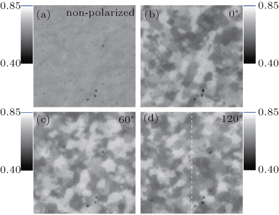 | Fig. 2. Transmittance images of a 50× 50 μ m2 region under non-polarized light (a), and polarized light of 0° (b), 60° (c), and 120° (d). |
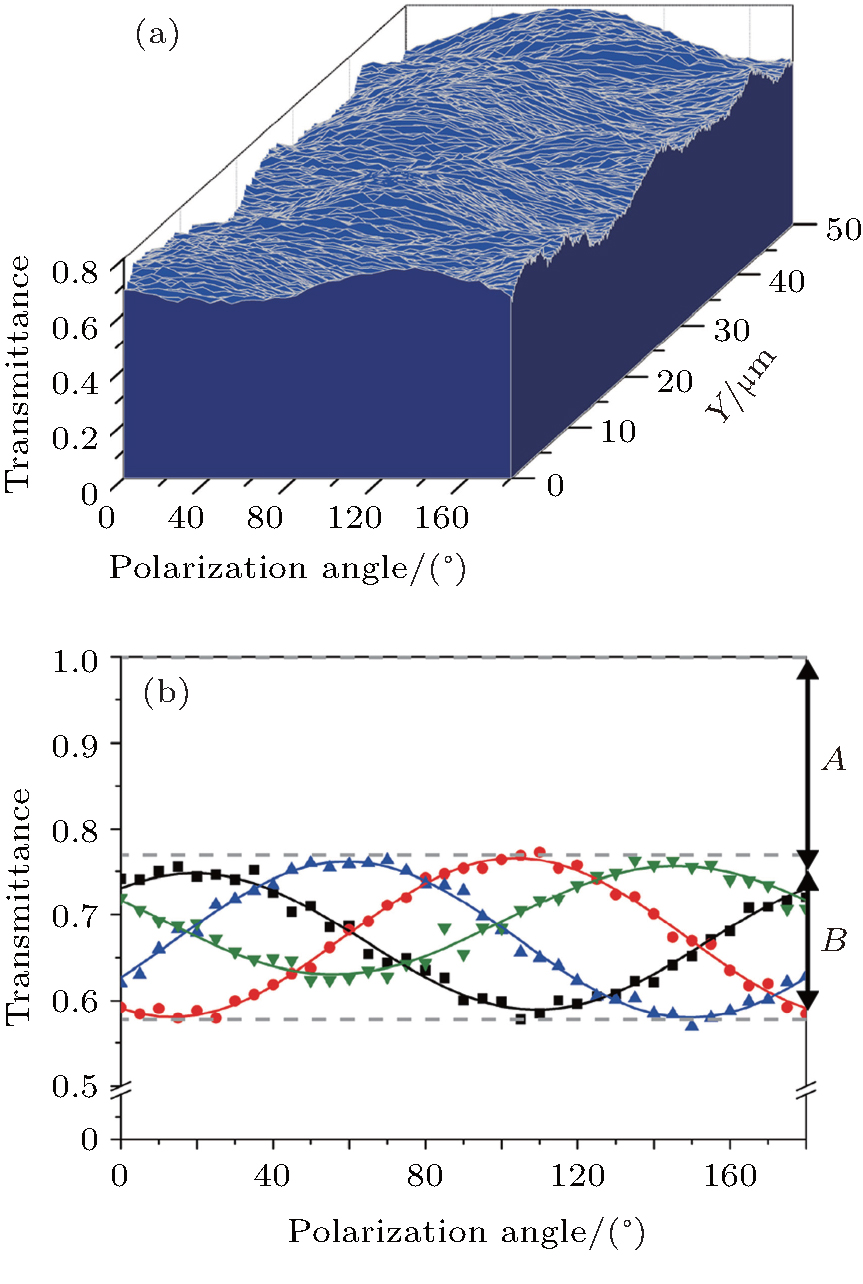 | Fig. 3. (a) Anisotropic transmittance curves of the pixels of a 50-μ m line. (b) Typical anisotropic transmittance curves (dots) fitted with a cosine function (solid lines), and the decomposition of the isotropic and anisotropic components is illustrated (dashed lines). |
are fitted with the cosine function derived from the model described above (see Section 2.2). The decomposition of the isotropic and anisotropic components can be clearly seen as indicated in the graph.
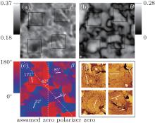
From the fitting of the model, values of the parameters A, B, and β can be derived. As described in the modeling of the transmittance (see Section 2.2), the crystallinity is reflected in the value of parameter B, and the relative orientation of the crystalline pattern is implied in the phase parameter β . To further demonstrate the meanings of the parameters, the anisotropic transmittance curves of all the pixels within a 22× 22 μ m2 region are fitted with the transmittance model. Subsequently, images of the parameters are drawn from two-dimensional arrays of the fitted values of A, B, and β as shown in Figs. 4(a)– 4(c). The isotropic component distribution of this region is contained in the image of A (Fig. 4(a) in gray scale); the relative crystallinity distribution is mapped in the image of B (Fig. 4(b) in gray scale); and the relative orientation distribution is reflected in the images of β (Fig. 4(c) in color). As seen in the image of β , pixels with the same or close β values are clustered in domains and the boundaries between divisive β values can be observed clearly. Therefore, the domains must correspond to ZnPc crystal grains, inside each of which the structural orientation is consistent, and the boundaries correspond to crystal grain boundaries. Hence, the distribution of crystal grains is directly resolved in the image of β . Meanwhile, the image of B shows that the crystallinity is higher inside large crystal grains, while it is much lower at grain boundaries. However, as implied in the model (see Section 2.2), the meanings of the values of B and β are relative, and the determination of their absolute meanings requires full information of the arrangement of the TDMs in the sample. Alternatively, references could be used in practical cases.
 | Fig. 4. (a) Isotropic component image drawn from fitted values of A. (b) Relative crystallinity image drawn from fitted values of B. (c) Relative orientation image drawn from fitted values of β . (d) AFM images (5× 5 μ m2 each) of the sub-regions of the 22× 22 μ m2 region indicated by the hollow squares in panels (a)– (c). |
Selected-area AFM images are acquired to confirm the parameter images and serve as absolute references. The four areas selected are indicated in each panel of Figs. 4(a)– 4(c) by hollow squares. The AFM images of these four areas are arrayed in Fig. 4(d) in the same sequence. As observed, the crystal grain and crystallinity distribution revealed in the AFM images are consistent with that revealed in images of β and B. With a higher spatial resolution, crystal needles inside crystal grains can be clearly distinguished in the AFM images. The needle directions of some crystal grains are marked with white arrows in Fig. 4(d). Correspondingly, the phase angles of these crystal grains are read from the image of β as shown in Fig. 4(c). While assuming a zero axis that is 42° clockwise from the polarizer zero axis, the orientations that the phase angles represent (indicated with white arrows in Fig. 4(c)) well match those needle directions distinguished from the AFM images. Hence, the AFM measurement confirms the validity of the model fitting and provides absolute orientation and crystallinity references to the fitted values.
Although the morphology information provided by our method can be obtained by AFM measurements with a higher spatial resolution, the high spatial resolution itself and the scanning mechanism of AFM make it very time-consuming to scan a large area. In contrast, the method we propose here, using transmission POM, provides a fast and convenient way to acquire morphological properties of WEG ZnPc films including crystal grain size, distribution, orientation, and crystallinity. This method can be readily generalized to reflection measurement and to other organic polycrystalline films or even inorganic polycrystalline films, as it does not depend on specific crystal structures. The large-scale imaging capacity of optical microscopy makes it very suitable for the study of organic thin-film electronics, the scale of which usually falls in micrometers to millimeters. Moreover, the good extendibility of optical microscopy makes it possible to incorporate POM with other kinds of measurement, e.g., incorporating electrical measurements to explore the micro-scale anisotropic electrical property of organic films. These capacities of the method could make it a highly efficient tool for both scientists and technicians.
As the application of organic electronics gains speed, the method we propose may pave a pathway to a low cost, efficient solution to the morphology checking procedure of the mass production of organic thin-film electronics. Once the values of crystallinity parameter B and orientation parameter β of a POM system are calibrated, by AFM or a standard sample for example, the system could work continuously as a morphology monitoring system. With the advantage of high-speed, large-scale, and all-optical imaging, full-range non-destructive sample examination could be achieved.
By combining POM and a transition dipole model, morphological properties, including crystal grain size, distribution, relative orientations and relative crystallinity of polycrystalline WEG ZnPc films, were visualized. Further AFM measurements confirm the results and serve as absolute references to the relative orientations and relative crystallinity. Beyond WEG ZnPc films, this method can be readily applied to other organic or even inorganic polycrystalline films, thus providing a fast and convenient way for morphology inspection of thin films of these materials.
We thank Cao Wen-Bing and Meng Qing-Yu (Institute of Physics, CAS) for their help in POM measurement and Jin Ai-Zi and Zhang Hui-Zhen (Institute of Physics, CAS) for their assistance in the AFM imaging. We are deeply grateful to Wang Zhuan and Li Yun-Liang (Institute of Physics, CAS) for their valuable comments and discussions.
| 1 |
|
| 2 |
|
| 3 |
|
| 4 |
|
| 5 |
|
| 6 |
|
| 7 |
|
| 8 |
|
| 9 |
|
| 10 |
|
| 11 |
|
| 12 |
|
| 13 |
|
| 14 |
|
| 15 |
|
| 16 |
|
| 17 |
|
| 18 |
|
| 19 |
|
| 20 |
|