Gu Min, Zhang La-Bao, Kang Lin, Zhao Qing-Yuan, Jia Tao, Wan Chao, Xu Rui-Ying, Yang Xiao-Zhong, Wu Pei-Heng, Zhang Yong, Xia Jin-Song. High efficiency, large-active-area superconducting nanowire single-photon detectors. Chinese Physics B, 2015, 24(6): 068501
Permissions
High efficiency, large-active-area superconducting nanowire single-photon detectors
Gu Mina), Zhang La-Baoa), Kang Lina)†, Zhao Qing-Yuana), Jia Taoa), Wan Chaoa), Xu Rui-Yinga), Yang Xiao-Zhonga), Wu Pei-Henga), Zhang Yongb), Xia Jin-Songb)
Research Institute of Superconductor Electronics (RISE), School of Electronic Science and Engineering, Nanjing University, Nanjing 210093, China
Wuhan National Laboratory for Optoelectronics and School of Optical and Electronic Information, Huazhong University of Science and Technology, Wuhan 430074, China
Niobium nitride superconducting nanowire single-photon detectors were fabricated on thermally oxidized silicon substrates with large active areas of 30 μm × 30 μm. To achieve non-constricted detectors, we improved the film growth and electron beam lithography process to fabricate uniform 100-nm wide NbN nanowires with a fill factor of 50%. The devices showed 72.4% system detection efficiency (SDE) at 100-Hz dark count rate (DCR) and 74-ps timing jitter, measured at the fiber communication wavelength of 1550 nm. The highest SDE which is 81.2% when the DCR is ∼700 c/s appears at the wavelength of 1650 nm.
Keyword:
85.25.Pb; 07.57.Kp; 85.60.Gz; single photon; superconductor; nanowire
Since Gol’ tsman fabricated ultrathin narrow niobium nitride (NbN) strips and a quantum efficiency of about 20% for 810-nm wavelength photons and low dark counts in 2001, [1] a lot of studies have been done for superconducting nanowire single-photon detectors (SNSPDs) because of their high system detection efficiencies (SDEs) and low dark counts ranging from visible to infrared wavelengths.[2– 5] This has shown that SNSPDs have many potential applications in quantum communication, quantum optics, classical laser communication, and time-of-flight ranging.[6, 7] In order to make SNSPDs play a great role in these fields, many remarkable studies have been done in recent years, committed to improving the system detection efficiency with low DCR and timing jitter.[6, 8– 11] In these works, although some SNSPDs incorporated arrays that contained three or even four detectors, the total active areas of the SNSPDs were small, ranging from 1.03 μ m × 1.14 μ m to 15 μ m × 15 μ m.[6, 8– 11] Due to the size of the active areas, single-mode fibers with a thin fiber core are often used in SNSPDs systems. The diameter of the light spot from single-mode fibers is 9 μ m or 10 μ m. A larger active area would make the light spot focus and couple on SNSPDs more easily. The research of Shigehito Miki et al. showed that larger active areas can achieve higher optical coupling efficiency for SNSPD devices.[12] Because of their high capacity and low cost, multimode fibers are widely used in the communications business, e.g., in local area networks, but they have larger core diameters. A large active area can also make possible the use of SNSPDs with multimode fibers. Due to their benefit for optical coupling, larger active areas also have specific applications in fields that require detecting irregularly emitted photons, such as infrared spectroscopy and bioluminescence technology. However, the fabrication of a large active area device is limited by the uniformity and the superconducting properties of the ultrathin films used for fabricating SNSPDs, which are dependent upon the crystal phase of the films and affected by crystal defects.[13, 14] This shows that the film growth process is crucial to the fabrication of SNSPDs with large active areas. Although it is difficult to fabricate SNSPDs with large active areas, some researchers have focused on it and did some work because of the great potential applications. Shigehito Miki fabricated 20 μ m × 20 μ m area SNSPDs with 80-nm and 100-nm linewidths and 50% fill factor on single-crystal MgO substrate. Since there was no cavity structure, the fiber-coupled detection efficiency of the devices was 0.4%– 3.5% at a 100-Hz dark count rate. They also found that the limitation for fabricating SNSPDs with large active areas was the constriction of the nanowires caused by defects in the superconducting film or introduced during nanofabrication. This means the deposit of films is so important.[15] Zhang et al. and Ejrnaes et al. have also done some experiments or theoretical calculation respectively for SNSPDs with large active areas.[16, 17] Dengkuan Liu et al. have fabricated SNSPDs with an active area 35 μ m in diameter; however, it works with high efficiency only at visible wavelengths.[18]
In the present paper, we present the fabrication of high performance ultrathin NbN SNSPDs with a large active area of 30 μ m × 30 μ m on thermally oxidized Si substrates, and the total length of the nanowire is about 4.5 mm. Then in a practical GM cryocooler system, we measured the SDE, DCR, timing jitter, and spectral characteristics of our device at 2.4 K.
2. Device design and fabrication
Figure 1 shows the simulated structure of SNSPDs consisting of a double-side cavity structure with back-side illumination. We simulated the absorption spectrum of the cavity using the commercial software, Finite-Difference-Time-Domain (FDTD). We assumed a three-dimensional unit cell consisting of Si substrate, SiO2, NbN nanowires, SiOx, and an Au mirror, from bottom to top, in the simulation. The periodic boundary condition was used in the x and y directions of the cavity structure and a perfectly matched layer (PML) boundary condition was used in the z direction. The incident light was assumed to be polarized parallel to the nanowires and to enter the device from the Si substrate. As the NbN nanowires were set to be ultrathin, general mesh generation does not meet our needs for calculation. In order to obtain accurate calculation results, we refined the mesh in a simulation area around each of the NbN nanowires, which was 1 nm along each of the x-, y-, z-axis directions, respectively.
Fig. 1. Three-dimensional (3D) Schematic diagram of fabricating an SNSPD device with a double-side cavity. The NbN nanowire width was 100 nm. The thickness of the SiO2, SiOx, and Au mirror layers were 250 nm, 240 nm, and 150 nm.
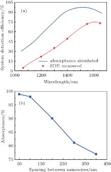
In our simulation, the line width of the NbN nanowire was set to 100 nm and its thickness was 6 nm. The thickness of the Au mirror was set 150 nm to ensure that light was perfectly reflected. We calculated for cavity structures with different thicknesses of SiO2 and SiOx layers and found that the optimal geometric parameters of the SiO2 and SiOx layers are 250 nm and 240 nm, respectively, at a wavelength of 1550 nm. The refractive indices used in the simulation are nSi = 3.478, nSiO2 = 1.444, nSiOx = 1.48, nNbN = 4.905 + i4.293, and nAu = 0.52 + i10.652.[11] Figure 2(a) gives the simulation results (the blue line) for the structural SNSPD described above, with 100-nm width and 100-nm spacing at wavelengths ranging from 1050 nm to 1650 nm. It shows clearly that the highest absorptivity value appears at the wavelength of 1550 nm. Figure 2(b) shows a simulation result of how the optical absorption in the nanowires depends on spacing between the nanowires with 1550-nm wavelength incident light. As shown in Fig. 2(b), the highest value of optical absorption is 98.9% at the closest spacing of 50 nm. With the filling factor reduced to 50% (100-nm spacing), the value of optical absorption decreases to 98%. With the spacing increasing, the optical absorption decreases monotonically and rapidly. The absorption drops to 77% for the nanowires with a large spacing of 400 nm. This shows that the absorption would be higher with closer spacing when the nanowire is 6-nm thick. When the incident light illuminates the device, the photons will transmit along the z axis stably back and forth in the optical cavity until they are absorbed by the NbN nanowires. However, each reflection at the interfaces of the cavity results in a loss of unabsorbed photons. This indicates that reducing the reflection can result in less loss and higher efficiency. A higher filling factor of the NbN nanowires means that NbN nanowires occupy more space, which causes higher absorption when unabsorbed photons pass through NbN nanowires after each reflection. This leads to less reflection and higher efficiency, which conforms to the simulation shown in Fig. 2(b). Although the absorption is higher with closer spacing, such fabrication would be more difficult to achieve. When the spacing is 50 nm, the fabrication of nanowires with large area is hardly achieved. The value of optical absorption decreases by only 0.9% with the spacing changing from 50 nm to 100 nm. Considering all factors in the simulation and process conditions, we chose the spacing of 100 nm for our devices in the experiment.
NbN thin films were deposited by reactive DC magnetron sputtering in a mixture of Ar and N2 gases at ambient temperature. The target was 99.999% pure niobium and the target was 6 inches (1 inch = 2.54 cm) in diameter, which made the uniformity of NbN films great. This was so important for fabricating nanowires with large active areas. We deposited 6-nm-thick NbN films, controlled by the deposition rate and deposition time. The zero resistance superconducting transition temperature of these films is above 7.5 K, which is very high for 6-nm thick NbN films deposited on thermally oxidized silicon substrates.
After the NbN films had been deposited, they were given 100-nm wide 100-nm spaced meander lines by direct e-beam lithography (EBL) and reactive ion etching (RIE), which covered a square active area of 30 μ m × 30 μ m. Finally, a 240-nm thick SiOx layer and a 150-nm thick Au mirror were fabricated to cover the nanowires by PECVD and RF sputtering in that order, at low temperature. This can enhance the efficiency of absorbing photons to the meandering area of a nanowire.
Fig. 2. (a) Simulation (blue line) and measurement (red line) results of SSPD device with 100-nm width and 100-nm spacing for wavelengths ranging from 1050 nm to 1650 nm. (b) Simulated spacing dependence of the optical absorptance in the 6-nm thick NbN nanowire.
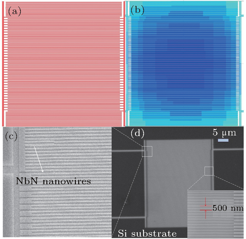
During the device fabrication process, the most important part is the fabrication of NbN nanowires by EBL to make the nanowires uniform with a sharp edge in these large areas. In order to obtain uniform nanowires fast, we used high acceleration voltage up to 100 kV to decrease the effect of backward scattering.[19] As resist thickness is a function of the development process, a thin resist layer could be used to get higher resolution.[20] So a layer of PMMA 70-nm thick was spun in our experiment. Besides the normal methods above, we did proximity effect correction and added dummy strips around the sensitive area to minimize the variations of exposure doses over a large pattern. Figure 3(a) shows a sketch of NbN nanowires we designed for EBL. We simulated the coming dose using a Monte Carlo method. As shown in Fig. 3(b), the result showed that the exposure dose should be varied during the process. We also changed the shapes of the nanowires with the intent to reduce the proximity effect. Due to the proximity effect, the nanowires at the corner were easily narrowed in EBL. As the critical current of the device was limited by the width of the narrowest nanowires, this would decrease the detection efficiency of the device. We made the corner of nanowires into a semicircle to correct the proximity effect. This avoided overexposing the corner of the nanowires. Finally, to avoid the nanowires in the boundary having different width from those in the central part, we extended some nanowires with some extra lines of the same width on both sides of the active area. This could make nanowires in the active area uniform as shown in Fig. 3. As shown in Fig. 3(b), the active area of nanowires fabricated in the central part had almost the same color (blue), which meant they were fabricated at the same doses. This made the nanowires in the boundary of the active area and in the central position have the same uniformity, which is very important for critical current of devices and device yield. Figure 3(d) presents SEM images of a fabricated NbN meander line with a large active area of 30 μ m × 30 μ m. The inset shows that the nanowire is straight with a width of 100 nm and spacing of 100 nm. This indicates that the NbN nanowires fabricated by EBL have a uniform width and regular intervals over an active area of 30 μ m × 30 μ m, and the total length of the NbN nanowires is up to 4.5 mm. Figure 3(c) shows the image of NbN nanowires and the extensional lines. We can find that nanowires are uniform and sharp by use of an extensional line in the EBL fabrication.
Fig. 3. (a) Sketch of nanowires designed for EBL. (b) Image of simulation result for computing the required applied doses to correct the proximity effect. (c) Image of NbN nanowires and the extensional lines. (d) Image of meandered NbN nanowires taken by SEM. It presents SEM images of a fabricated NbN meander line with its active area as large as 30 μ m × 30 μ m. The inset shows that the nanowire is straight with a width of 100 nm and spacing of 100 nm.
3. Measurement and results discussion
To measure our fabricated SNSPDs, we put the device in a compact package using a fiber with a focusing lens to obtain good optical coupling efficiency between the incident light and active area of the device. By changing the distance between fiber and device chip, the spot size of incident light on the active area was about 9 μ m. The packaged device was installed into a GM cryocooler system. In this system, the device was cooled down to 2.4 K with a thermal fluctuation range of 10 mK. Semi-rigid coaxial cable and single mode fiber were introduced to the package. The semi-rigid coaxial cable was connected with a bias tee and a room temperature low noise amplifier outside the cryocooler.
For measuring the SDE, a 1550-nm wavelength pulsed laser with a 100-fs pulse width was used as an input photon source and it was attenuated heavily so that the photon flux illuminating the device was 2.5 × 10⁵ photons/s, which was sufficiently low to keep the linearity of the output counts for the incident photon flux as we did before.[16, 21, 22] A fiber polarization controller was also used to control the polarization properties of the incident photons to maximize the SDE. When measuring the spectral characteristics, a continuously tunable system consisting of a xenon lamp (wavelength ranging from 200 nm to 2500 nm) and a monochromator was used to supply illumination light of different wavelengths to the device. SNSPD output counts were measured by a pulse counter. The time jitter characteristics were measured by using a time-correlated single-photon counting module with a 1-ps resolution (HydraHarp 400, PicoQuant GmbH).
3.1. System detection efficiency, dark count rate, and spectral characteristics
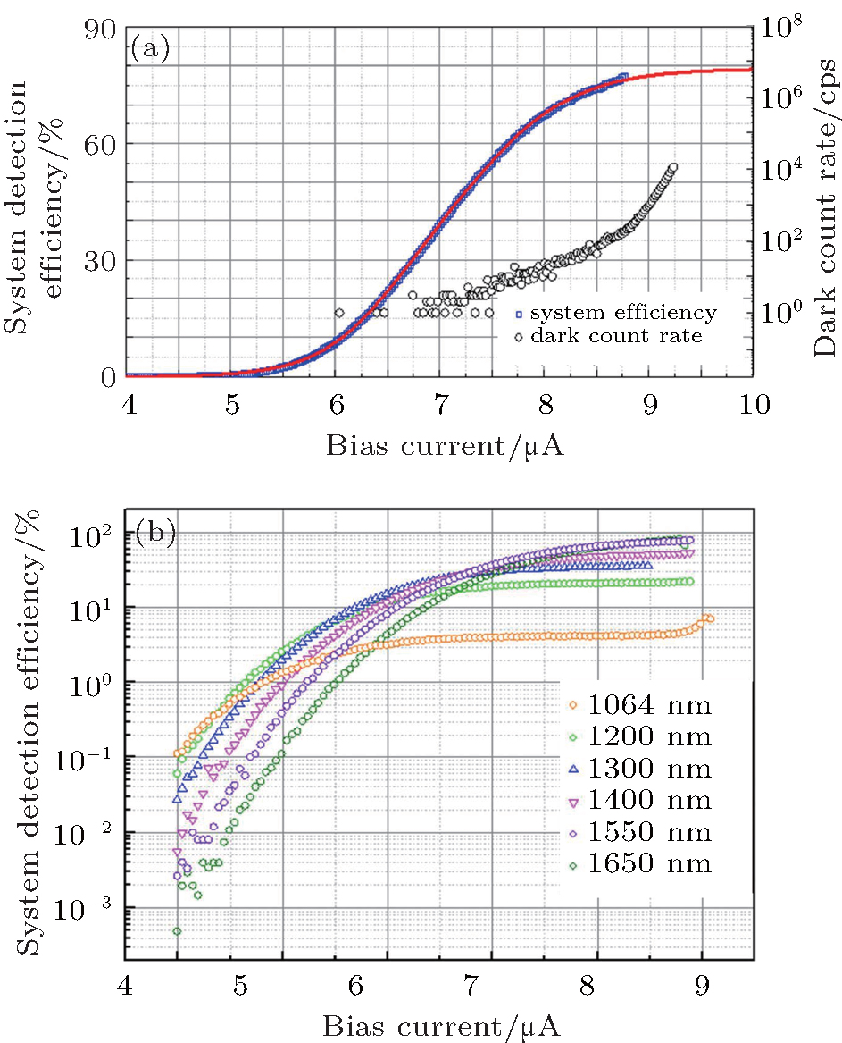
Figure 4(a) shows the measured bias current dependencies of SDE (blue hollow square points) and DCR (empty circles). The SDE was 72.4%, when DCR was 100 c/s under a bias current of 8.3 μ A, at 1550-nm wavelength, and the measured maximum SDE (SDEmax) was 77.2% at the DCR of ∼ 600 cps under a bias current of 8.73 μ A. This shows that the SDE curve of this device has not saturated, and we fitted the SDE data by a sigmoid function, shown as the red line in Fig. 4(a). This shows that the potential maximum SDE of this device is 79.1% by fitting.
Figure 4(b) shows the SDE of the device at different wavelengths ranging from 1064 nm to 1650 nm. As shown clearly, the SDE curve at a wavelength of 1064 nm (orange line) quickly attained saturation as bias current increased, because the energy of a photon with a shorter wavelength is higher than it is with a longer wavelength when it can be easily absorbed to excite response pulse by nanowires. This also shows that the highest measured SDE appears at the wavelength of 1650 nm, which is 81.2% when the DCR is ∼ 700 c/s. Although we designed the device intending the peak of SDE to be at the wavelength of 1550 nm, the highest measured SDE appeared at the wavelength of 1650 nm due to the thickness deviation generated in the thermal oxidation process and the PEVCD process. To compare the experimental result and numerical simulation, the measured SDEs of the device and the fitting curve are shown in Fig. 2(a) (the red dots and line) with wavelengths ranging from 1064 nm to 1650 nm when the DCR is 100 c/s. The highest value appears between the wavelengths of 1550 nm and 1650 nm owing to the thickness deviation generated in thermally oxidized process and PEVCD process. This also shows that the SDEs measured around the wavelength of 1550 nm are much higher than those far from 1550 nm, which is caused by the thickness of the cavity, and it is in accord with our design. From the image, we can find the trends of the two lines are the same, but the SDEs measured are lower than simulated absorption efficiencies. The most probable reason is that a small part of the photons absorbed by NbN nanowires did not excite response pulses or the response pulses were not read by the readout circuit. Other reasons such as coupling efficiency would also lead to a measured SDE being lower than the simulated absorption efficiency. Also, a device working in a lower temperature environment can show a better measured SDE.[6]
Fig. 4. (a) System detection efficiency (SDE) and dark count rate versus bias current for 6-nm thick SNSPDs with a 30 μ m × 30 μ m active area of 100-nm width nanowires spaced at 100 nm. The SDE was 72.4% with DCR of 100 c/s under a bias current of 8.3 μ A, at 1550-nm wavelength, and the measured maximum SDE (SDEmax) was 77.2% at the DCR of ∼ 600 cps. The potential maximum SDE of this device is 79.1% evaluated from fitting by a sigmoid function. (b) The SDE of the device at different wavelengths ranging from 1064 nm to 1650 nm. The highest SDE measured, which is 81.2% when the DCR is ∼ 700 c/s appeared at the wavelength of 1650 nm.
3.2. Response pulse and timing jitter
Figure 5(a) shows oscilloscope traces of the response pulse of the SNSPD biased at IB = 8.3 μ A, when DCR is about 100 cps. The decay time of the response pulse of the SNSPD (τ ) is about 194 ns, which is a little longer due to the length of the nanowires.[9] The length of the nanowires was about 4.5 mm, which is much longer than nanowires in previous SNSPD studies. The kinetic inductance (Lk) of SNSPD can be estimated by fitting the falling edge of a pulse with the equation of
where A is the highest value of the pulse, t0 is the corresponding time for the highest value of the pulse, and R is 50 Ω . The inset in Fig. 5(a) gives the falling edge of the pulse (blue line) and the fitting curve (red line). By fitting the pulse, we can estimate that our device with 4.5-mm nanowires has Lk of 3.97 μ H, which is only twice as large as it is in a conventional 50%-filling-factor device with 1.406-mm long nanowires.[11] Figure 5(b) shows the timing jitter observed at a bias current of 8.3 μ A. The full width at half maximum (FWHM) of the timing jitter is 74 ps.
Fig. 5. Reset time and timing jitter. (a) The oscilloscope traces of the response pulse of the SNSPD biased at IB = 8.3 μ A, when DCR is about 100 cps. The decay time of the SNSPD (τ ) was defined as the time required for the pulse to decay from 90% to 10% of the maximum of the pulse (red arrows). The inset image gives the falling edge of the pulse (blue line) and the fitting curve (red line). (b) Histogram of timing jitter.
4. Conclusion
In conclusion, we have presented a 6-nm thick NbN SNSPD device with a large active area of 30 μ m × 30 μ m. It showed a system DE as high as 72.4% at a wavelength of 1550 nm at DCR of 100 c/s and timing jitter of 74 ps. We also measured the SDE at different wavelengths ranging from 1064 nm to 1650 nm, and found the measured highest SDE was 74.9% with the DCR of 100 cps at a wavelength of 1650 nm. The results show that SNSPDs with large active areas have various possible applications in different areas. In the future, we hope to achieve the application of multimode fibers on our SNSPDs with large active areas.
Gol’tsmanG N, OkunevO, ChulkovaG, LipatovA, SemenovA, SmirnovK, VoronovB, DzardanovA, WilliamsC and SobolewskiR2001Appl. Phys. Lett. 79705[Cited within:1][JCR: 3.794]
2
ZhangL B, KangL, ChenJ, ZhaoQ Y, JiaT, XuW W, JinB B and WuP H2011Acta Phys. Sin. 60038501(in Chinese)[Cited within:1][JCR: 1.016][CJCR: 1.691]
3
WangY J, DingT, MaH Q and JiaoR Z2014Chin. Phys. B23060308DOI:10.1088/1674-1056/23/6/060308[Cited within:1][JCR: 1.148][CJCR: 1.2429]
4
GuM, KangL, ZhangL B, ZhaoQ Y, JiaT, WangC, XuR Y, YangX Z and WuP H2015Chin. Phys. Lett. 32038501DOI:10.1088/0256-307X/32/3/038501[Cited within:1][JCR: 0.811][CJCR: 0.4541]
... tsman fabricated ultrathin narrow niobium nitride (NbN) strips and a quantum efficiency of about 20% for 810-nm wavelength photons and low dark counts in 2001,[1] a lot of studies have been done for superconducting nanowire single-photon detectors (SNSPDs) because of their high system detection efficiencies (SDEs) and low dark counts ranging from visible to infrared wavelengths ...
1
2011
1.016
1.691
... [2#cod#x2013 ...
1
2014
1.148
1.2429
1
2015
0.811
0.4541
1
2014
1.148
1.2429
... 5] This has shown that SNSPDs have many potential applications in quantum communication, quantum optics, classical laser communication, and time-of-flight ranging ...
4
2013
3.546
0.0
... [6,7] In order to make SNSPDs play a great role in these fields, many remarkable studies have been done in recent years, committed to improving the system detection efficiency with low DCR and timing jitter ...
... [6,8#cod#x2013 ...
... [6,8#cod#x2013 ...
... [6] ...
1
2006
3.794
0.0
... [6,7] In order to make SNSPDs play a great role in these fields, many remarkable studies have been done in recent years, committed to improving the system detection efficiency with low DCR and timing jitter ...
2
2011
13.025
0.0
... [6,8#cod#x2013 ...
... [6,8#cod#x2013 ...
1
2013
27.254
0.0
... [9] The length of the nanowires was about 4 ...
1
2013
3.546
0.0
4
2013
3.546
0.0
... 11] In these works, although some SNSPDs incorporated arrays that contained three or even four detectors, the total active areas of the SNSPDs were small, ranging from 1 ...
... 11] Due to the size of the active areas, single-mode fibers with a thin fiber core are often used in SNSPDs systems ...
... [11] Figure#cod#x00A0 ...
... [11] Figure#cod#x00A0 ...
1
2011
0.0
0.0
... [12] Because of their high capacity and low cost, multimode fibers are widely used in the communications business, e ...
1
2009
2.758
0.0
... [13,14] This shows that the film growth process is crucial to the fabrication of SNSPDs with large active areas ...
1
2011
0.71
0.0
... [13,14] This shows that the film growth process is crucial to the fabrication of SNSPDs with large active areas ...
1
2008
3.794
0.0
... [15] Zhang et al ...
2
2009
1.782
0.0
... [16,17] Dengkuan Liu et al ...
... [16,21,22] A fiber polarization controller was also used to control the polarization properties of the incident photons to maximize the SDE ...
1
2009
0.0
0.0
... [16,17] Dengkuan Liu et al ...
1
2014
3.546
0.0
... [18] ...
1
1999
0.0
0.0
... [19] As resist thickness is a function of the development process, a thin resist layer could be used to get higher resolution ...
1
2001
1.267
0.0
... [20] So a layer of PMMA 70-nm thick was spun in our experiment ...
1
2009
0.0
0.95
... [16,21,22] A fiber polarization controller was also used to control the polarization properties of the incident photons to maximize the SDE ...
1
2011
1.782
0.0
... [16,21,22] A fiber polarization controller was also used to control the polarization properties of the incident photons to maximize the SDE ...
High efficiency, large-active-area superconducting nanowire single-photon detectors
[Gu Mina), Zhang La-Baoa), Kang Lina)†, Zhao Qing-Yuana), Jia Taoa), Wan Chaoa), Xu Rui-Yinga), Yang Xiao-Zhonga), Wu Pei-Henga), Zhang Yongb), Xia Jin-Songb)]


 , Zhao Qing-Yuan