High efficiency, large-active-area superconducting nanowire single-photon detectors

High efficiency, large-active-area superconducting nanowire single-photon detectors |
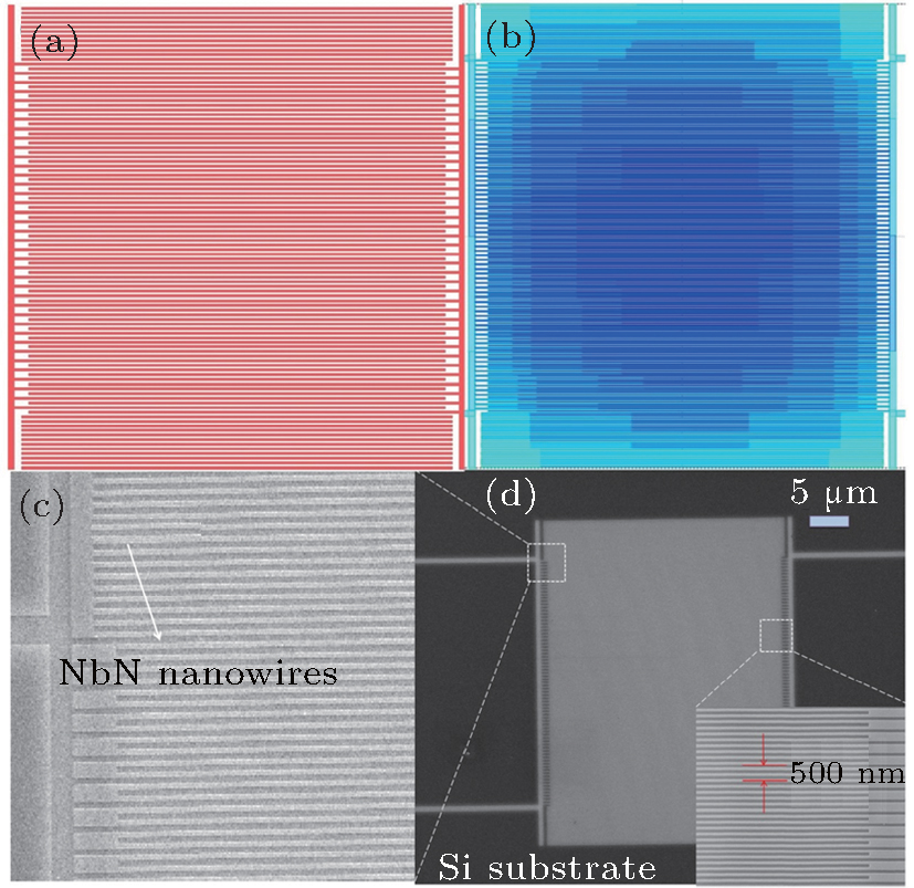
| (a) Sketch of nanowires designed for EBL. (b) Image of simulation result for computing the required applied doses to correct the proximity effect. (c) Image of NbN nanowires and the extensional lines. (d) Image of meandered NbN nanowires taken by SEM. It presents SEM images of a fabricated NbN meander line with its active area as large as 30 μm × 30 μm. The inset shows that the nanowire is straight with a width of 100 nm and spacing of 100 nm. |
 |