
Characterization of CoPt nanowire fabricated by glancing angle deposition
[Satoshi Kitaia), b)†  , Zhang Zheng-Jun
a) , Shi Jib) , Yoshio Nakamurab) ]
, Zhang Zheng-Jun|
|


†Corresponding author. E-mail: kita.s.aa@m.titech.ac.jp
CoPt and Co nanowire films were deposited by the Glancing Angle Deposition (GLAD) method. All samples are deposited on Si substrates that were covered by polystyrene spheres to assist the alignment of nanowires. SEM observation results show that the length and diameter of nanowires are uniform for all samples. According to the result of XRD, the crystal structure of CoPt is fcc. The angular dependence of magnetization of the nanowires shows that the easy axis of magnetization is along the growth direction of the nanowires.
In recent years, magnetic recording media has played an important role in the information world. Especially, perpendicular magnetic recording media has been successfully applied in hard disc drives after decades of intensive study. CoPt alloy film with an L10-ordered structure has been regarded as a promising perpendicular magnetic recording media for its high anisotropy energy and chemical stability.[1] On the other hand, one-dimensional structures such as nanorods or nanowires have also attracted great interest in recent years because of their unique properties such as mechanical strength, [2, 3] photoluminescence, [4] and magnetic properties.[5, 6] The practical application of such materials is a very interesting topic among researchers. Especially magnetic nanowire materials have been considered to have great application potential as high-density magnetic material.[7] Magnetic nanowire has strong shape anisotropy and matrices of such nanowires are suitable for high-density, low noise and high thermal stability magnetic memory materials. Intensive researches have been conducted by using various fabrication methods.[8, 9] It is considered that if the crystal anisotropy of CoPt and the shape anisotropy of nanowire superimpose with each other, a CoPt nanowire matrix will be a very promising material for magnetic recording.[10] Electrodeposit on the anodic aluminum oxide (AAO) is considered as a promising way to fabricate such a structure.[11– 19] In such studies, CoPt shows strong anisotropy energy and its length, diameter, and inter-wire distance are important factors for anisotropy energy.[15, 20] Meanwhile, some problems of this method have also been reported. For example, when removing the anode from the surface of the substrate as post treatment, the uniaxial magnetic anisotropy disappeared.[21] Moreover, it is difficult to obtain the single crystal phase by this method.[22] There have been some reported works conducted to overcome these problems.[21, 23– 25]
In this research, we fabricated CoPt rod-like structures by the Glancing Angle Deposition (GLAD) method. GLAD can be used to prepare nanowire materials by controlling oblique angle and substrate rotation speed.[26] The oblique angle causes a shadowing effect and produces a column structure, while the substrate rotation speed controls the shape of the column, such as zigzag, helix, and vertical columns. Length and composition rate are important factors to determine the magnetic properties of CoPt nanowire, and they can be controlled easily for this method. So in this part of work, we change the length and composition rate of samples and study the magnetic properties of the sample.
All samples were deposited on Si substrates that were covered with hexagonal close-packed polystyrene spheres (PS). The diameter of PS is 200 nm for all samples. The following equation shows the relationship between the diameter of nanowires and the oblique angle, a diameter of PS[27]

where d is the diameter of the nanowire, r is the radius of the PS, and α is the oblique angle. According to the equation, the diameter of the nanowire is determined by the oblique angle. The larger oblique angle and smaller radius of the PS lead to a smaller diameter of nanowires. The length/diameter ratio is also an important factor for the shape anisotropy of magnetic nanowires. In this part of work, the oblique angle of the sample is set at 87° , which is the largest oblique angle for our instrument.
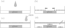
All Si substrates were cleaned in boiling Piranha solution (4:1 (v/v) H2SO4/H2O2) for 1 hour in order to promote the alignment of polystyrene spheres, and thus the alignment of CoPt nanowires. The Si (100) wafers were degreased by ultrasonic cleaning in acetone, ethanol, and deionized water for 1 h before deposition. A specific method was used to obtain close-packed monolayer PS.[27] The PS solution (10 wt%) was diluted with deionized water and then mixed with ethanol (4.2:5 (v/v)). The mixture was ultrasonicated for 30 min to ensure the uniform dispersing of the PS spheres. The fabrication process is shown in Fig. 1. The glass plate was put on the center of a petri dish (D = 15 cm), and filled with deionized water until the height of the water level was slightly higher than the glass plate. Then the PS solution was dropped on the glass plate and the PS diffused on the water surface as shown in Fig. 1(b). After the water was covered by the PS solution, sodium dodecyl sulfate (SDS) was added, making the PS sphere align densely to form a closed packed monolayer. Finally, we carefully slide Si substrates into the water until the water was completely dried up. A uniform layer of PS then formed on the surface of Si substrates after drying.
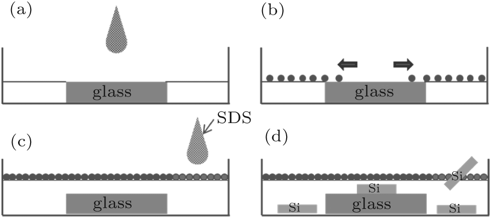 | Fig. 1. Process for preparing Si substrate covered with polystyrene sphere. (a) Dropping the PS solution on the glass plate. (b) PS diffused on the surface of the water. (c) Dropping SDS solution. (d) Sliding Si substrate into the water. |
Nanowires of Co and CoPt are prepared by using a dc magnetron sputtering apparatus. Figure 2 shows the formation process of nanowires on PS spheres. All samples are prepared at room temperature. The base pressure in the chamber is 2.0 × 10− 4 Pa. To understand the effect of Pt content in the nanowire, three kinds of targets were used for this work. Pure Co target (99.999% purity), with 40% of its surface covered by Pt plates, are used to prepare Series 1 samples. For Series 2 samples, 70% of the surface of the Co target was covered by Pt plates. To compare the difference of characteristics between conventional deposited film and nanowire films, conventional films were deposited under the same conditions for 90 min for each composition. Sputtering was carried out at 9.0 × 10− 1 Pa, the discharge current and voltage during sputtering is 0.32 A at 0.32 kV for Co target and 0.4 A at 0.24 kV for the Co– Pt target. The sputtering time is 60, 90 min for Series 1, 60, 75, 90 min for Series 2, and 60, 90, 120 min for Pure Co. Samples are named in the order of deposition time as #1, #2, for Series 1, #3, #4, #5 for Series 2, and #6, #7, #8 for Pure Co. To investigate the effect of annealing, the samples were annealed at 300, 400, 500, 600 ° C for 1 hour in an Ar atmosphere. A scanning electron microscope (SEM) was used to investigate the morphology of all samples, and x-ray diffraction (XRD) for structure characterization. To analyze the composition of samples, inductively coupled plasma-mass spectrometry (ICP-MS) and an electron probe micro analyzer (EPMA) were used for all samples. The magnetic properties of samples were investigated by a vibrating sample magnetometer (VSM). All samples were handled by Teflon tweezers to avoid a contamination of magnetic materials.
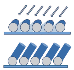 | Fig. 2. Schematic diagram of glancing angle deposition with polystyrene sphere. |
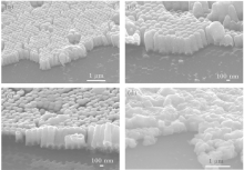
The length of the nanowires is controlled by the deposition time. Figure 3 shows the SEM images of the samples. It can be seen that tilted well-aligned nanowires have been obtained. Due to the high oblique angle of the substrate, the geometric shadowing effect occurs (see Fig. 2), leading to the deposition of uniform and well-aligned nanowires. The polystyrene sphere self-assembled into a colloidal monolayer on the Si substrate, leading to the high alignment of nanowires.[28] Many results have been reported about synthesis CoPt nanoparticles which can be used for magnetic memory devices.[1] However, the random size of nanoparticles is a main disadvantage in view of the practical applications of this material.[29] One of our objectives of this research is to solve this problem by using GLAD with polystyrene spheres. From the SEM observation, we can clearly see that all the nanowires grow on the polystyrene spheres. Some researchers have already reported that the nanowire deposited by this method has high-alignment and uniform length and diameter.[26, 30– 33] According to Eq. (1), the nominal diameter of nanowire is about 180 nm, and the actual diameter is from 150 nm to 170 nm. If the oblique angle is smaller, the diameter is larger, so it can be considered that the actual oblique angle may be slightly smaller than 87° for the samples. The length and length/diameter ratio of all samples are shown in Table 1. The diameter of nanowire is almost the same for all samples and its value is 160 nm. Inter-wire distance is also an import factor for practical use of magnetic memory devices. One single-domain nanowire is expected to correspond to one bit-cell because of its high shape anisotropy energy. It has been reported that the large size distribution and the inter-wire distance would reduce the squareness of the hysteresis loop.[5] The nanowire prepared in this research was grown by the shadow effect of polystyrene spheres, so the inter-wire distance is determined by the diameter of the polystyrene spheres and the tilted angle of GLAD. Polystyrene spheres are aligned as a closed-packed structure, so the inter-wire distance of these nanowires is very small, which is about 10– 20 nm for all samples. The tilt angle of nanowires is about 35° for all samples. Figure 3(c) shows the cross-section view of the #5 sample. The nanowires are tilted with the same angle, and it can be seen that the length and diameter of nanowire are uniform.
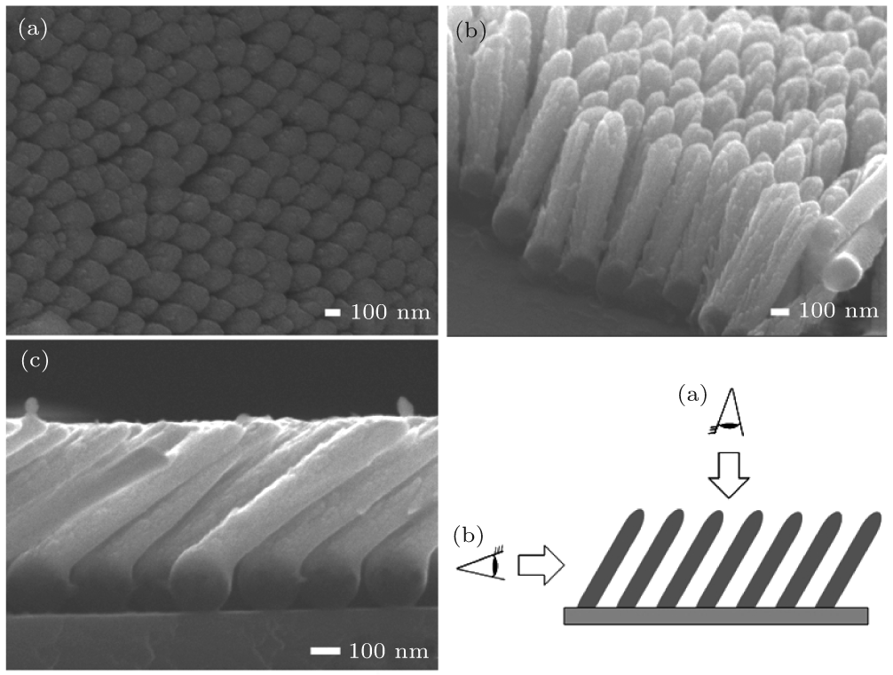 | Fig. 3. SEM images of the #5 samples. (a) Top view of #5 sample; (b) and (c) cross-section view of the same sample. |
| Table 1. Structure and magnetic property of CoPt nanowires. |
For magnetic materials, the ordering transformation of the crystal structure is a very important factor for magnetic properties. However, morphology changes might occur during the annealing. Hence, we try to find the best temperature of annealing for this material. Figure 4 shows the SEM images of #5 after annealing. We can see that after annealing at 300 ° C and above, polystyrene spheres are completely melted and disappear, but nanowires still stand on the substrate up to 400 ° C. At 500 ° C, the nanowires merge into large grains. Nanowires completely disappear at 600 ° C. This might be caused by the crystal growth during annealing. Thus, 400 ° C is the highest temperature of annealing for those samples.
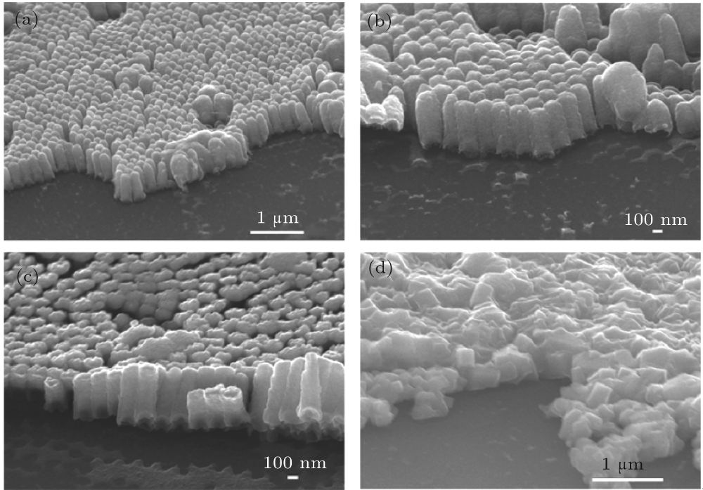 | Fig. 4. SEM images of #5 after annealing. (a) 300 ° C, (b) 400 ° C, (c) 500 ° C, and (d) 600 ° C. |
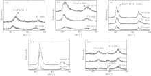
The XRD results of all samples are shown in Fig. 5. Figures 5(a) and 5(b) show the results of Series 1 and Series 2 before annealing. CoPt (111) and (200) peak can be confirmed in both series. Therefore, the crystal structure of these samples is fcc. Other researchers also reported[34] that CoPt films deposited by a magnetron sputtering system form fcc crystal structure. As mentioned above, we conducted annealing for both series of samples. Figure 5(c) shows the XRD result of Series 2 after annealing. The two peaks from the fcc CoPt can be confirmed at around 41° and 47° . The peak intensity increases with increasing deposition time. Both peaks shift to a high angle direction after annealing, indicating the change of stress/strain in the CoPt nanowires.
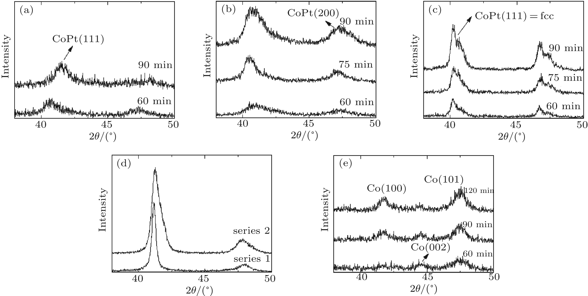 | Fig. 5. XRD profiles of the samples. (a) Series 1, (b) Series 2, (c) annealed samples of Series 2, (d) a conventional film, and (e) the pure Co nanowire. |
The conventional CoPt films without nanowire structures of the two series also show the (111) texture, as can be confirmed from Fig. 5(d). On the other hand, the XRD results of Co nanowire contain Co (100), (002), and (101) peaks from the hcp structures. This means the crystal structure of Co nanowire is hcp.
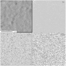
The EPMA and ICP-MS measurements are conducted for all samples. The EPMA mapping shows that Co and Pt atoms were distributed uniformly in all samples. As shown in Fig. 6, the upper left is an SEM image of #5 sample, and the other images are the distribution of Si (substrate), Co, and Pt. One can see the uniform distribution of Co and Pt in the film. It is reported that by using the electrodeposit method, nanowires have uniform length and diameter, but their composition lacks uniformity.[35] Our results indicate that a sample prepared by magnetron sputtering has a very uniform composition. Table 1 shows the composition of all samples. The average content of Pt in #1 and #2 is about 11%, and that in #3– #5 is about 42%. The results of ICP-MS show similar results to the EPMA.
 | Fig. 6. Results of the EPMA of #5. |
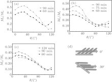
The nanowires prepared in this study are 35° tilted for all samples. To know the easy axis of nanowires, angular dependence of remanent squareness of all samples has been investigated.[13, 36] Figure 7 shows the angular dependence of samples in each series. The results show that the highest value of remanet squareness of the samples is around 30° and the lowest value is at around 120° . The angle for the highest value is quite close to the tilted angle of nanowires, which means that the easy axis of nanowires is along their growth direction. The lowest value is obtained at around 120° , indicating that this is perpendicular to the growth direction of nanowires. Similar results can be obtained for all samples. Magnetic coercivity slightly increases for Series 2, but there is no angular dependence for all samples. Hc is reported to decrease with increasing wire diameter, which can be explained by the curling model.[9] In this study, the diameter of nanowire is almost the same for all samples. Therefore, the angular dependence of coercivity cannot be confirmed in this study.
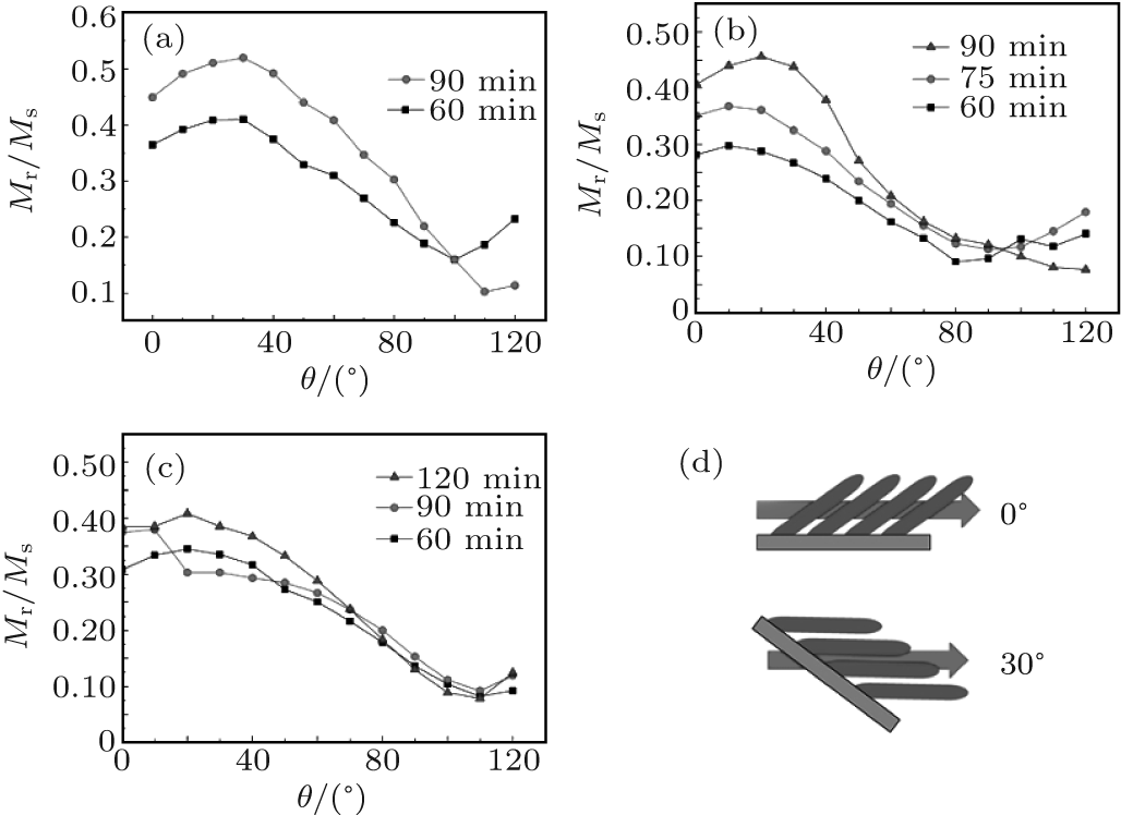 | Fig. 7. Angular dependence of Mr/Ms. (a) Series 1, (b) Series 2, (c) Pure Co. (d) Schematic of measuring direction. |
The results of CoPt conventional film explain that CoPt is strongly magnetized in the in-plane direction and its Hc is smaller than nanowire samples. This result is similar to the results of previous researches[37] and the small value of coercivity confirms that CoPt has an fcc structure.
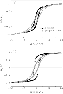
The saturated field differences (Δ Hs = Hs∥ – Hs⊥ ) are also compared for all samples. Δ Hs is the important factor to investigate the alignment of easy axis. Here Hs∥ is the saturation field when the magnetic field is applied parallel to the nanowire axis and Hs⊥ is the saturation field when the magnetic field is applied perpendicular to the nanowires axis. When the value of Δ Hs is negative, it means that the magnetic easy axis is parallel to nanowire.[38] In this work, the direction shows that the highest Mr is defined to be parallel to the nanowire axis and the lowest Mr is defined to be perpendicular to the nanowire axis. The results are shown in Table 1. In this study, Δ Hs of all samples shows negative values, which means the magnetic easy axis is parallel to the growth direction for the samples. The value of – Δ Hs increases with increasing the length of nanowire. CoPt can have the L10 crystal structure, which has a high magnetic anisotropy energy (2.8 × 10⁷ g/s2· cm) and its magnetically easy axis is along the c axis. In this research, we could not confirm the formation of the L10 ordered phase in the present work. On the other hand, the crystal anisotropy has strong dependence on the measurement temperature, while the shape anisotropy does not.[39] Hence, the VSM measurement was conducted at low temperature (4 K) to confirm the major source of anisotropy. Figure 8 compares the magnetization curves measured at room temperature and low temperature. We could not confirm significant difference between low temperature and room temperature measurements in both easy axis and hard axis. This again confirms that the majority of anisotropy energy is the shape anisotropy in our nanowire films. The highest – Δ Hs value is obtained at Co 120 min. This sample is the longest sample and its shape anisotropy energy is the highest in this research.
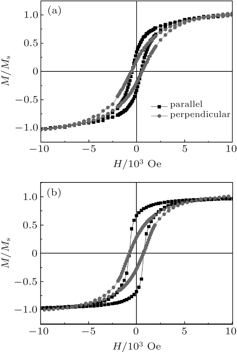 | Fig. 8. Magnetic curves of samples. (a) Series 2 #5 at room temperature. (b) The same sample at low temperature. |
The CoPt and Co nanowires are prepared by GLAD. All samples are deposited on Si substrates covered with polystyrene spheres with a diameter of 200 nm. The inter-wire distance and diameter of nanowires are uniform for all samples, and the values are 10– 20 nm and 160 nm, respectively. The XRD results show the crystal structure of CoPt is fcc before and after annealing. The average Pt content is 11.3% for Series 1 and 42.5% for Series 2. The magnetic properties of samples show that the easy axis of samples is parallel to nanowires, and remanent squareness and – Δ Hs are increased by increasing the length of nanowire. Magnetic properties at low temperatures confirm that the anisotropy energy of nanowire is mainly from the shape anisotropy.
The authors wish to express appreciation to the Tokyo Tech-Tsinghua Joint Graduate Program, Tsinghua University for use of the experimental devices and Tokyo Institute of Technology for research suppot.
| 1 |
|
| 2 |
|
| 3 |
|
| 4 |
|
| 5 |
|
| 6 |
|
| 7 |
|
| 8 |
|
| 9 |
|
| 10 |
|
| 11 |
|
| 12 |
|
| 13 |
|
| 14 |
|
| 15 |
|
| 16 |
|
| 17 |
|
| 18 |
|
| 19 |
|
| 20 |
|
| 21 |
|
| 22 |
|
| 23 |
|
| 24 |
|
| 25 |
|
| 26 |
|
| 27 |
|
| 28 |
|
| 29 |
|
| 30 |
|
| 31 |
|
| 32 |
|
| 33 |
|
| 34 |
|
| 35 |
|
| 36 |
|
| 37 |
|
| 38 |
|
| 39 |
|