†These authors contributed equally to this work.
‡Corresponding author. E-mail: zhbaij@mail.sysu.edu.cn
*Project supported by the National Natural Science Foundation of China (Grant Nos. 61274039 and 51177175), the National Basic Research Program of China (Grant Nos. 2010CB923201 and 2011CB301903), the Ph.D. Program Foundation of Ministry of Education of China (Grant No. 20110171110021), and the Foundation of the Key Technologies R&D Program of Guangdong Province, China (Grant No. 2010A081002005).
Crack-free GaN/InGaN multiple quantum wells (MQWs) light-emitting diodes (LEDs) are transferred from Si substrate onto electroplating Cu submount with embedded wide p-electrodes. The vertical-conducting n-side-up configuration of the LED is achieved by using the through-hole structure. The widened embedded p-electrode covers almost the whole transparent conductive layer (TCL), which could not be applied in the conventional p-side-up LEDs due to the electrode-shading effect. Therefore, the widened p-electrode improves the current spreading property and the uniformity of luminescence. The working voltage and series resistance are thereby reduced. The light output of embedded wide p-electrode LEDs on Cu is enhanced by 147% at a driving current of 350 mA, in comparison to conventional LEDs on Si.
Over the last two decades, GaN-based LEDs on sapphire and SiC substrates have been applied in many fields, such as displays, traffic signals, automotive lighting, and backlights. This is due to the rapid development of the LED technologies.[1– 13] Specifically, the progress in achieving internal quantum efficiency improvement and radiative efficiency enhancement, [2, 14, 15] hole transport improvement and efficiency-droop suppression in the LEDs leading to practical applications, [16– 21] and the deep understanding of Auger process in nitride LEDs[22, 23] have been the driving force in advancing the technologies. In order to further reduce the cost of LEDs and replace traditional lamps, the LEDs on Si substrates have attracted considerable interest, owing to many good properties of Si such as low cost, large scale, high quality, low hardness, and good thermal conductivity and electrical conduction. Although GaN-based LEDs on Si substrates have been extensively studied and their performances have been improved greatly, the volume production remains difficult mainly due to the stress problems between GaN and Si substrate and the optical absorption by the opaque Si substrate. The stress problems can be partially solved by using graded AlGaN buffer layers[24, 25] and AlN/GaN superlattices.[26, 27] In order to improve the light efficiency, inserting a distributed Bragg reflector (DBR) between the active layer of LED and the substrate is an easy and effective method for reducing the absorption of Si substrate.[28– 30] However, because of the tensile stress and the crack formation, only a few pairs of DBRs are available to be deposited on Si substrates in the premise of crackfree, which results in lower reflectivity. Moreover, only a given light polarization impinging near the normal direction to the DBR structure can be effectively reflected.[31] In addition, DBRs are usually applied in conventional p-side-up LEDs, which cannot eliminate the shadow effect by p-electrodes.[32] Therefore, the Si substrate transferring technique[33– 40] is mainly adopted to eliminate the absorption of Si substrates and shadow effect, by inserting a metallic reflector. For instance, in our previous work, [40] we presented the embedded electrode LEDs (EE-LEDs) transferred from Si substrate onto Cu submount, which enhances the light output by 122%. However, since the p-electrode is much narrower than the TCL and the thin TCL presents lateral resistance, it leads to current crowding near the p-electrode, [40, 41] which would also aggravates the shadow effect in the conventional p-side-up LEDs. This current crowding adversely affects the uniformity and stability of the light emission.[42] Moreover, the current crowding also causes optical saturation, decrease in the efficiency of light generation, and degradation in the reliability of LEDs, due to the high-electrical carrier density in a localized area of the device.[43] Consequently, we widen the embedded p-electrode to cover almost the whole TCL in this study, which improves the current spreading property and the uniformity of luminescence, and reduces the working voltage and the series resistance of the LEDs on Cu. Besides these improvements, the shadow effect of p-electrode is eliminated in this n-side-up LED structure. Measured by high-resolution X-ray diffraction (HR-XRD), the LEDs transferred from Si substrate onto Cu submount show almost fully residual strain relaxation in the film, which results in a reduction of quantum confined stark effect (QCSE) and an enhancement of internal quantum efficiency (IQE). In addition, the rough surface of embedded wide p-electrode LEDs on Cu is beneficial for light extracting, because of the configuration with AlN seeding layer facing up. Together with the removal of opaque Si substrate, the inserting of metallic reflector and the electroplating of Cu submount, performance of embedded wide p-electrode LEDs on Cu exhibits significant improvement.
Growth details of LEDs on Si substrates by metal organic chemical vapor deposition (MOCVD) method were presented in our previous work.[40] Figure 1 shows the device fabrication processes of the embedded wide p-electrode LEDs on Cu. (i) The wafer was etched to form LED mesas and through-holes by the inductively coupled plasma reactive ion etching (ICP-RIE) system, as shown in Fig. 1(a). (ii) Ni/Au (5/7 nm) metals were deposited onto the p-GaN layer to serve as a TCL, and annealed at 570 ° C for 15 min. Subsequently, Cr/Pd/Au (20/40/200 nm) metals were deposited to form the wide p-electrodes, covering almost the whole TCL. During this process, these metals were also used to fill the through-holes, forming n-electrodes, as shown in Fig. 1(b). The p- and n-electrodes were annealed at 200 ° C in N2 ambient. (iii) The p- and n-electrodes were isolated by depositing an insulator, followed by Cr/Al/Pd/Au metals as a metallic reflector, whose reflectivity in the blue spectrum range is 65%– 70%. Then, a 100-μ m-thick electroplating Cu layer was served as a submount, as shown in Fig. 1(c). (iv) The wafer was bonded to a temporary substrate using an acrylate adhesive. Then, the Si substrate is thinned to 100 μ m, as shown in Fig. 1(d). (v) The Si substrate was removed by wet-chemical etching in HNA (HF:HNO3:CH3COOH= 1:1:1) solutions. Then the n-electrode metal filled into the through-holes and the AlN seeding layer were exposed, as shown in Fig. 1(e). (vi) Finally, the acrylate adhesive was washed off and the devices were separated from the temporary substrate. Figure 1(f) illustrates the schematic diagram of the embedded wide p-electrode LED on Cu with the chip size of 1× 1 mm2, which shows an n-side-up and vertical-conductive configuration.
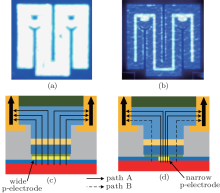
The electroluminescence (EL) measurements of the wide p-electrode and the narrow p-electrode LEDs were performed, and their light-emitting images are shown in Figs. 2(a) and 2(b), respectively. It is clearly seen that the wide p-electrode LED exhibits good uniformity of luminescence, while the narrow p-electrode region of the narrow p-electrode LED is much brighter than other emission regions. The reasons are demonstrated by Figs. 2(c) and 2(d). Benefitting from the wide p-electrode covering almost the TCL, the current spreading capacity is significantly improved, as shown in Fig. 2(c). The improved current spreading property thereby results in good uniformity of luminescence. Nevertheless, due to the lateral resistance of the thin TCL, [41] most currents are confined near the narrow p-electrode, as shown in Fig. 2(d). In addition, we also find that the contact resistances of metallic reflector/TCL and metallic reflector/p-electrode/TCL are 1.235 Ω and 0.81 Ω , respectively. The former is 52% larger than the latter, which is caused by the contact resistance of the unalloyed metallic reflector and the generation of NiOx after alloy of Ni/Au TCL. These resistances are averse to the current spreading, which leads to current crowding effect near the narrow p-electrode. This current crowding adversely affects the uniformity and stability of the light emission. Moreover, the current crowding also leads to optical saturation, decrease in the efficiency of light generation, and degradation in the reliability of LEDs, due to the high-electrical carrier density in a localized area of the device.
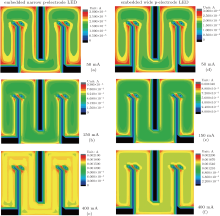
In order to further investigate current spreading properties affected by the width of p-electrodes, current distribution simulation is performed by the P simulation program with integrated circuit emphasis (PSPICE) software. Figure 3 shows simulated current distributions of the active layers of the embedded wide p-electrode and the narrow p-electrode LEDs under different injecting currents of 50, 150, and 400 mA, respectively. Figures 3(a) and 3(d) illustrate that the current distributions show no obvious difference for these two LEDs when injecting smaller current. However, when increasing the injecting current, the current distributions of these two LEDs are quite different. As shown in Figs. 3(b) and 3(c), the current crowding effect of the narrow p-electrode LED becomes serious, especially near the narrow p-electrode and the edge. On the contrary, the wide p-electrode LED exhibits quite good uniformity of current distribution, which benefits from the significantly improved current spreading capacity by the wide p-electrode covering almost the whole TCL, as shown in Figs. 3(e) and 3(f). These results correspond well with the EL measurements.
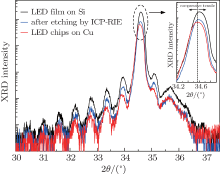
The crystalline quality and the variation stresses during the fabrication of the embedded wide p-electrode LEDs on Cu are characterized by HR-XRD. Figure 4 shows the 2θ /ω scans around GaN (0002) of the LED wafer on Si before and after etching by ICP-RIE, and the embedded wide p-electrode LED on Cu, respectively. The satellite peaks can be observed clearly in those samples, which indicates that no obvious deteriorations are found in the MQWs after the LEDs transferred from Si substrate onto Cu. The diffraction peaks of GaN (0002) are shown in the inset of Fig. 4. According to the 2θ values, the LED on Si shows a tensile stress. While after the Si substrate removal, an almost fully strain relaxation is observed in the embedded wide p-electrode LED on Cu. This strain relaxation is in favour of the reduction of QCSE and the enhancement of IQE.
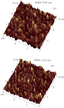 | Fig. 5. Surface morphologies of (a) the conventional LED on Si and (b) the embedded wide p-electrode LED on Cu measured by AFM at an area of 3× 3 μ m2. |
Figure 5 shows the surface morphologies of the conventional LED on Si and the embedded wide p-electrode LED on Cu measured by atomic force microscopy (AFM) at an area of 3× 3 μ m2, respectively. Compared with the conventional LED on Si, the embedded wide p-electrode LED on Cu exhibits much larger root mean square (RMS) of roughness, which results from the exposed AlN seeding layer of the n-side-up vertical-conductive configuration. The rougher surface can consequently enhance the light extraction efficiency (LEE).
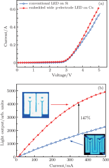
To further investigate the electrical and the optical properties of the embedded wide p-electrode LED on Cu submount and the conventional LED on Si substrate, injecting current versus voltage (I– V) and light output versus injecting current (L– I) characteristics were measured, as shown in Fig. 6. The forward voltage at 350 mA and series resistance of the embedded wide p-electrode LED on Cu are 4.22 V and 3.1 Ω , respectively. While those of the conventional LED on Si are 4.43 V and 3.8 Ω , respectively, as shown in Fig. 6(a). That is to say, the former exhibits lower working voltage and smaller series resistance than the latter, which arises from the improved current spreading property by the widened p-electrode. Figure 6(b) shows that the light output of the embedded wide p-electrode LED on Cu is enhanced by 147% at a driving current of 350 mA, in comparison to the conventional LED on Si. The enhancement in light output is attributed to the increase of IQE and LEE. As described above, the embedded wide p-electrode LED on Cu shows a strain relaxation, which leads to an enhancement in IQE. The increase in the LEE is attributed to the following reasons. First, the opaque Si substrate was removed and the metallic reflector and Cu submount with better thermal conductivity were applied. Second, the embedded p-electrode was widened, which promoted current spreading, improved the uniformity of luminescence and reduced working voltage and series resistance. Third, the electrode-shadow effect was eliminated and the light extraction was increased by the rough surface of the exposed AlN seeding layer.
In summary, crack-free GaN-based embedded wide p-electrode LEDs were transferred form Si substrate onto the electroplating Cu submount. Compared with the previous work, the most important improvement was to widen the p-electrode, which significantly improved the current spreading property and the uniformity of luminescence, and thereby reduced working voltage and series resistance, although the reflectivity of the metallic reflector was weakened to some extent. As a consequence, the enhancement of the light output was increased from 122% to 147%. Moreover, the metallic reflector would be optimized and served as the p-electrode in our further work, which would not only increase the reflectivity but also improve the current spreading property. In a word, this device fabrication process showes no complexity, which is advantageous for improving the process reliability, increasing the yield, and further reducing the cost of LED chips.
| 1 |
|
| 2 |
|
| 3 |
|
| 4 |
|
| 5 |
|
| 6 |
|
| 7 |
|
| 8 |
|
| 9 |
|
| 10 |
|
| 11 |
|
| 12 |
|
| 13 |
|
| 14 |
|
| 15 |
|
| 16 |
|
| 17 |
|
| 18 |
|
| 19 |
|
| 20 |
|
| 21 |
|
| 22 |
|
| 23 |
|
| 24 |
|
| 25 |
|
| 26 |
|
| 27 |
|
| 28 |
|
| 29 |
|
| 30 |
|
| 31 |
|
| 32 |
|
| 33 |
|
| 34 |
|
| 35 |
|
| 36 |
|
| 37 |
|
| 38 |
|
| 39 |
|
| 40 |
|
| 41 |
|
| 42 |
|
| 43 |
|


