1. IntroductionZnTe is a semiconductor of the II– VI family with a zincblende structure and a direct energy gap Eg of 2.26 eV at room temperature, and has attracted growing attention because of its applications in green light emitting devices, THz detectors, wave guides, solar cells, and modulators.[1– 5] The epitaxial growth of ZnTe on GaAs has aroused considerable interest because GaAs is a desirable substrate due to its important role in the optoelectronic industry. If ZnTe could be grown epitaxially on GaAs, device integration would be possible.[5] However, the lattice mismatch and the difference in thermal expansion coefficient between the GaAs substrate and the ZnTe epilayer are considered to lead to strain and structural defects.[6, 7] Hence, to improve the structural quality of the ZnTe epilayer, various growth techniques concerning ZnTe/GaAs heterostructures have been explored, [8– 10] and some work has been done on the ZnTe epilayers grown on GaAs substrates by molecular beam epitaxy (MBE) and metal– organic vapor phase epitaxy (MOVPE).[5, 11, 12] Despite all that, compared with the study of homoepitaxial growth of ZnTe, the investigation of the heteroepitaxial growth of ZnTe on GaAs is still in its infancy. Therefore, more researches are needed before obtaining a high-quality ZnTe epilayer to meet the requirements for optoelectronic device applications.
MOVPE is a promising growth technique for obtaining epitaxial layers, and is suitable for mass production. Here, to obtain a high-quality ZnTe heteroepitaxial layer, a ZnTe epilayer grown on (100) GaAs substrate is prepared by using the MOVPE system under suitable growth conditions, [5, 13] while a ZnTe bulk crystal grown by the vertical Bridgman growth method is also presented for comparison. Photoluminescence (PL) measurement results from these two samples indicate that it is possible to fabricate a high-crystalline quality ZnTe heteroepitaxial layer by the MOVPE growth technique.
3. Results and discussionFigure 1(a) shows the PL spectra of the ZnTe epilayer in a range of 1.90 eV– 2.41 eV, measured at 6 K and 2 μ W. As seen from Fig. 1(a), the PL spectrum of the ZnTe epilayer is dominated by a sharp excitonic emission peak Ia at around 2.371 eV with a very narrow full-width at half maximum (FWHM) of about 1.5 meV. The spectrum is similar to that obtained from the ZnTe homoepitaxial layer on (100) ZnTe substrate.[14] The sharp emission peak Ia is attributed to the recombination transition of an exciton bound to the neutral-shallow-acceptors such as Li, Na, and Cu.[1, 5, 15] The peak (denoted as Ia-LO) on the low-energy side of the peak Ia by 26 meV, is a phonon replica of the peak Ia. It is worth noting that neither both the Y lines usually at 2.188 eV and 2.147 eV which are known to arise from extended structural defects, [16, 17] nor the oxygenbound- exciton (OBE) emission band at around 1.986 eV[18, 19] appears here. Likewise, neither the donor– acceptor pair (DAP) emission at around 2.329 eV which is due to the recombination transition between the Zn vacancy (VZn) acceptor and Te vacancy (VTe) donor or between the Zn interstitial (Zni) donor and the Te interstitial (Tei) acceptor, [20] nor VZn-related emission at around 2.355 eV, [21] is observed. The results indicate that the ZnTe epilayer structure is of good quality in terms of its crystallinity.
In order to observe clearly the main peak Ia and its excitation power-dependent behavior, figure 1(b) shows the enlarged PL spectra of the Ia peak shown in Fig. 1(a) at different excitation powers, and figure 2 shows the plots of the energy position and intensity of the peak Ia as a function of excitation power. With excitation power increasing from 2 μ W to 40 mW, it is seen from Figs. 1(b) and 2, that the Ia peak intensity increases due to the effective capture of the photo-generated carriers by the neutral-shallow-acceptors below the excitation power of about 10 mW, and then becomes gradually saturated. At the same time, the energy position of the peak Ia exhibits a slight red-shift with increasing excitation power. The energy redshift could be attributed to the increase in strain with the increase of the effective excited depth in the ZnTe epilayer.[22, 23] In fact, in previous work, [5] it has been found that the energy of the Ia peak increases monotonically with increasing ZnTe epilayer thickness, suggesting that a tensile strain existing in ZnTe/GaAs epilayer can be gradually relaxed with increasing the ZnTe epilayer thickness.
Figure 1(b) shows that on the high-energy side of the main peak Ia, a new emission peak (denoted by Ic) appears at a high excitation power. The peak Ic is considered as the transition of the excitons bound to the As atoms (or As-related complex) diffusing from the GaAs substrate into the epilayer during the growth of the epilayer, due to the high growth temperatures.[5] With increasing excitation power, the peak Ic markedly increases in intensity relative to the Ia peak, while a new free excitonic (FE) emission peak appears on the highenergy side of the Ic peak. In order to observe clearly the emission components at around 2.371 eV, the inset in Fig. 1(b) gives the further enlarged PL spectrum including the Ia, Ic, and FE peaks at 40 mW. The aforementioned behavior for the FE emission peak is due to the energy level filling of the ZnTe epilayer with the increase of the number of the photogenerated carriers. In contrast, however, the marked increase in the Ic peak intensity is mainly attributed to the rapidly increasing density of the As atom in the ZnTe epilayer with increasing effective excited depth. This is because the As atoms diffusing into the ZnTe epilayer are mainly distributed near the epilayer/substrate interface, [5, 24] and figure 1 shows the absence of the emission peak Ic in the low excitation range below 1 mW. This is also consistent with the result previously reported by the authors, i.e., the intensity of the Ic peak drastically decreases with increasing the epilayer thickness.[5] Therefore, it is believed that this problem could be solved by appropriately increasing the epilayer thickness.
Figure 3 shows the excitation power-dependent PL spectra of the ZnTe bulk crystal measured at 6 K. The PL spectra are dominated by an emission band (denoted by Ib) at around 2.340 eV in the low excitation range. In fact, as seen from Fig. 3 the emission band Ib contains two emission components: a low-energy component located at around 2.335 meV (denoted by Ibl) and a high-energy component at around 2.344 meV (Ibh). In addition, a weak emission band (denoted by Ib-LO) at around 2.314 eV is the phonon replica of the emission band Ib, and the weak peak at around 2.375 eV originates from the contribution of the emission Ia that may be due to the VZn.[20] Here, it should be pointed out that although the PL spectra of the ZnTe bulk crystal are dominated by the Ib emission in the low excitation range, the Ia emission from the ZnTe bulk crystal is stronger than that observed in the ZnTe epilayer in the same measurement conditions. The weaker Ia emission for the ZnTe epilayer may be due to the aforementioned As atoms diffusing from the GaAs substrate into the ZnTe epilayer, and/or because of the strain-induced degradation of the crystalline quality of the ZnTe epilayer. With the increase of excitation power in our measurement range, the emission peak Ia together with the well-resolved emission lines of the ground state FE(1S) and excited state FE(2S) of the free excitons, [25] shows a rapid increase in intensity compared with the emission band Ib, as expected. At the same time, the low-energy emission component Ibl shows a slower increase in intensity than the high-energy emission component Ibh (see inset, Fig. 3), while it gradually shifts towards the higher-energy side and partially merges into the high-energy emission Ibh. This is a typical characteristic of donor– acceptor pair (DAP) emission often observed in the spectra of the ZnTe bulks and ZnTe homoepitaxial epilayers.[26, 27] Consequently, the low-energy emission component Ibl is considered to be a DAP emission, which may result from the carrier transition between the Zn vacancy (VZn) acceptor and the Te vacancy (VTe) donor or between the Zn interstitial (Zni) donor and the Te interstitial (Tei) acceptor.[20] The aforementioned slower intensity increase and the clear peak blue-shift for the emission peak Ibl with increasing excitation power, are due to the gradual saturation of the PL components from distant pairs emitting in the low-energy part of the emission band Ibl.[28, 29] On the other hand, for the high-energy emission component Ibh, the peak blue-shift with increasing excitation power is less obvious. The aforementioned characteristics show that the emission component Ibh may originate from the conduction bandacceptor (e– A) emission.[28, 30] This less obvious peak blueshift for the emission Ibh with increasing excitation power, is due to the large state density for the conduction electron. For the type of emission component Ibh, this will be discussed later.
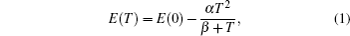
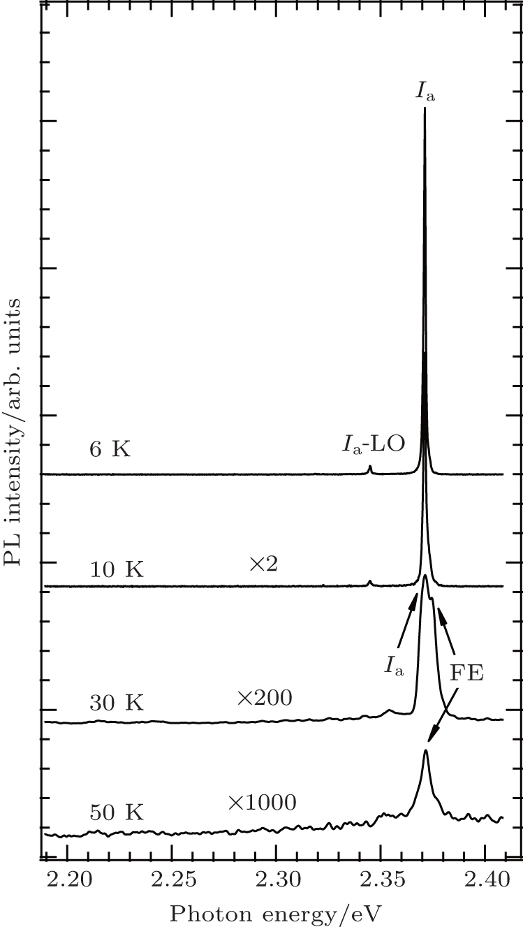
Figures 4 and 5 show the temperature-dependent PL spectra of the ZnTe epilayer and ZnTe bulk crystal measured at 1 mW, respectively. As seen from Figs. 4 and 5, the Ia emissions in both the structures have similar behaviors. That is, with increasing temperature, the intensity of the emission Ia rapidly decreases compared with those of the FE and Ibh emissions, reflecting the thermal dissociation process of the bound excitons from the neutral-shallow-acceptors. At the same time, the emission Ibl (i.e. the DAP emission) is rapidly quenched with increasing temperature (Fig. 5), due to the thermal release of electrons from the shallow donor to the conduction band.[28, 29]
Figure 5 also shows that, with increasing temperature, the peak position of the Ibh emission shows a blue-shift relative to those of the Ia and FE emissions. Figure 6(a) shows the typical temperature dependences of the peak energies of the emissions Ibh and FE(2S). The FE(2S) peak energy is associated with the band-gap energy, and can be found by subtracting its binding energy from the band-gap energy. That is, the variation of the FE(2S) peak energy is equal to that of the band-gap energy. The dashed curve in Fig. 6(a) represents a fit to the FE(2S) experimental data by using the Varshni equation[31]
with the following parameters: E(0) = 2.382 eV, α = 0.545 meV/K, and β = 203 K, where E(T) and E(0) are the FE(2S) emission energy at T and 0 K, respectively, and α and β are the Varshni coefficients. Figure 6(a) shows that the temperature dependence of the FE(2S) energy closely follows the Varshni equation. In contrast, however, the peak energy of the emission Ibh shows a slight blue-shift relative to the Varshni curve with increasing temperature.
As is well known, the peak energy of the FE transition is[30]

where EG and Ex are energy gap and binding energy of the free exciton, respectively. While the temperature dependence of the peak energy of the e– A transition can be written as

where EA is the acceptor binding energy, γ is a constant relating to the dimension of free electron motion in the ZnTe epilayer, k is the Boltzman constant, and kT is due to the kinetic energy and the energy dependence of the transition probability of free electrons.[30] Thus from Eqs. (2) and (3), the temperature dependence of the spectral peak separation between the FE and e– A transition lines, Δ E, can be written as

which shows that Δ E decreases linearly with temperature with the slope being γ k since EA and Ex are independent of temperature.
To identify the type of emission Ibh, i.e., whether the emission Ibh originates from the e– A emission, figure 6(b) shows the temperature dependence of the spectral peak separation (Δ E) between the FE(2S) and the Ibh transition lines. The slope obtained from the least-square fit between data points in Fig. 6(b) and Eq. (4) is about 0.57k (i.e. γ = 0.57). That is, with increasing temperature the emission component Ibh shifts towards the FE(2S) emission at a rate of 0.57k. This is a typical characteristic of the e– A emission often observed in GaN or GaN-based materials.[28– 30] Together with the observed excitation power dependence shown in Fig. 3, the emission component Ibh is considered to be of an e– A emission. The e– A emission may be due to the Zn vacancy (VZn), and/or Te interstitial (Tei). Figures 1– 5 also show that the emission Ia for the ZnTe epilayer has a lower peak energy of about 4 meV than that for the ZnTe bulk crystal. The reason for this is not clear now, but it may be due to the different acceptors for these two structures, or due to the tensile strain in the ZnTe epilayer induced by the lattice mismatch and the difference in thermal expansion coefficient between the GaAs substrate and the ZnTe epilayer.[5, 23]
All of these results show that both the ZnTe epilayer and the ZnTe bulk crystal used in this work are of good structural quality, due to the sharp bound excitonic emission Ia and the absence of deep structural defect-related Y lines. Furthermore, although the excitonic emissions (Ia and FE) from the ZnTe epilayer are somewhat weaker than that from the ZnTe bulk crystal, which may be due to As atoms diffusing into the ZnTe epilayer and/or because of the strain-induced degradation of crystalline quality of the ZnTe epilayer, the DAP and e– A emissions, which are observed in the ZnTe bulk crystal in this work or are often observed in the ZnTe bulk crystal and ZnTe homoepitaxial layers in other studies, [26, 27] do not appear in the ZnTe epilayer, indicating that the ZnTe epilayer grown on its GaAs substrate is a promising material or structure for applications in future optoelectronic devices. It is believed that by further optimizing the growth process, such as using the patterned substrates and low-temperature nucleation layers, introducing the strain release layers, and optimizing the growth parameters (temperature, reactor pressure, and transport rate), these unfavorable factors (the tensile strain and the diffusion of the As atom from the GaAs substrate) affecting the quality of the crystallinity of the ZnTe epilayer could be rendered less harmful. Therefore, it is possible to obtain a high-quality ZnTe heteroepitaxial layer by using the MOVPE system, which is comparable to the ZnTe bulk crystal or ZnTe homoepitaxial layer.


 , Feng Zhi-Hong